12. Buck-Boost Converter#
In this lecture, we will start with the last basic topology of DC-DC converters, the review the basic calculations of all three topologies. In the end, we will have a tutorial for problem solving of three DC-DC topologies.
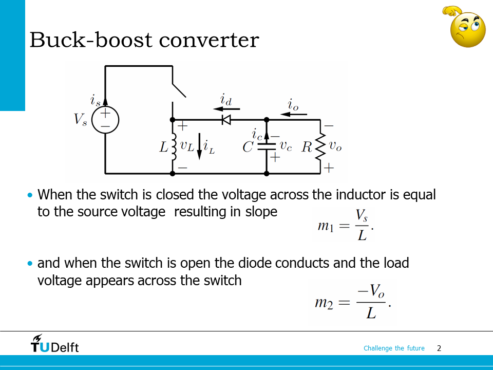
The topology for buck-boost converter is shown on the slide. Now the inductor is between the switch and the diode, while the diode polarity is reversed compared to the other topologies. As we studied briefly in the last part of Buck and Boost Conversion, the voltage transfer ratio can be solved from the current slopes during on and off through the inductor.
When the switch is closed, voltage across the inductor is the source voltage, so the current slope is \(m_1 = \frac{V_s}{L}\).
When the switch is open, the diode is forward biased, so the load voltage appears across the switch, the current slope becomes \(m_2 = \frac{-V_o}{L}\), or \(m_2 = \frac{-V_c}{L}\), since the output voltage ripple is negligible.
Attention
Pay attention to the positive polarity definition of the output voltage in the schematic above, which is different from the previous case in Buck and Boost Conversion.
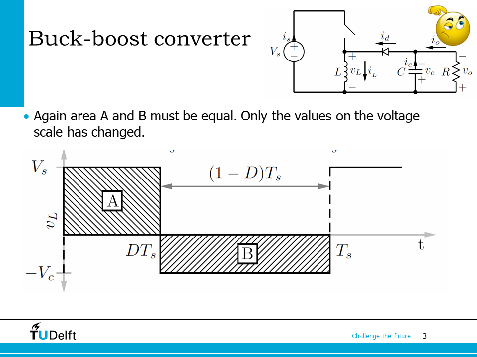
Based on the steady state assumption, in CCM, we know
or in other words, the two shadowed areas A and B should be equal, then we have
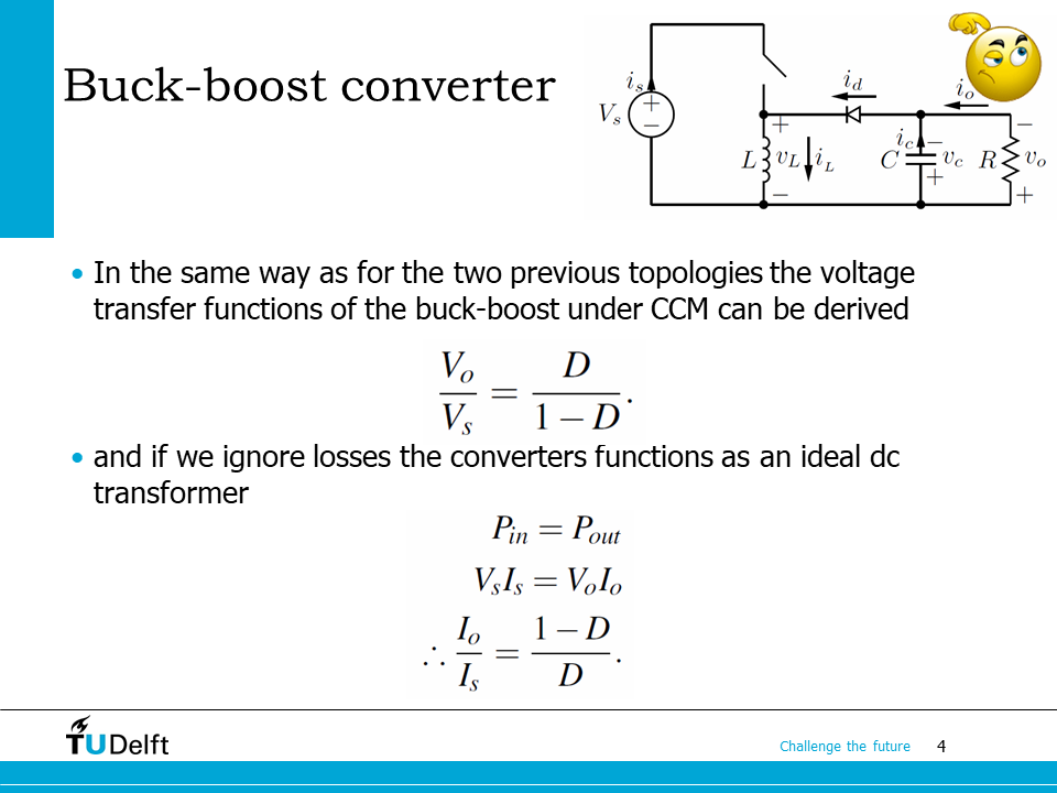
Once the voltage transfer ratio is derived, from the power balance and ideal component assumption, we know the current transfer ratio is exactly the inverse of it
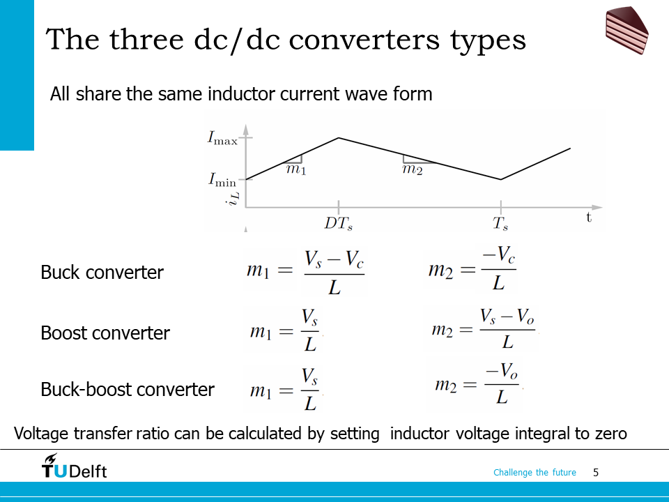
It can be seen that in CCM, the inductor current waveforms in the three topologies (buck, boost, buck-boost) all show the same triangular shape. The current slopes during on and off are summarised on this slide. The voltage transfer ratio can then be calculated by applying the steady state assumption, i.e., by setting the inductor voltage integral in one switching cycle to be zero, or by equalising the \(\Delta i_L\) calculated from the two slopes during the on and off periods.
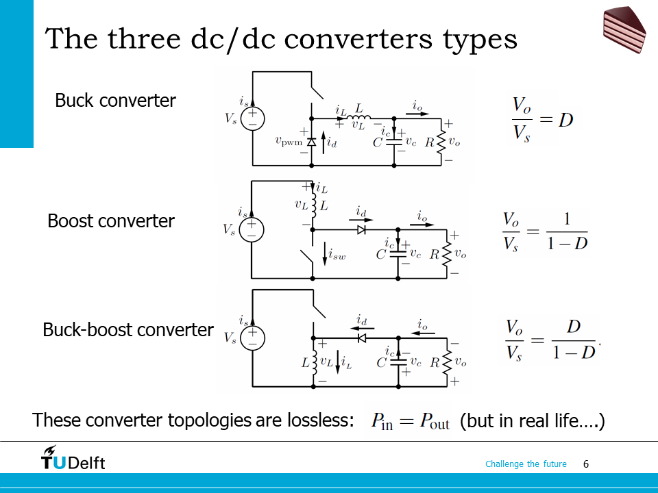
The voltage transfer ratios are summarised here. If ideal components are used, the three converter topologies can be considered to be lossless, so the current transfer ratio is just the inverse of the voltage ratio. However in real life, all components: inductor, semiconductor switch, diode and capacitor, have losses, so the efficiency will be always below 1.
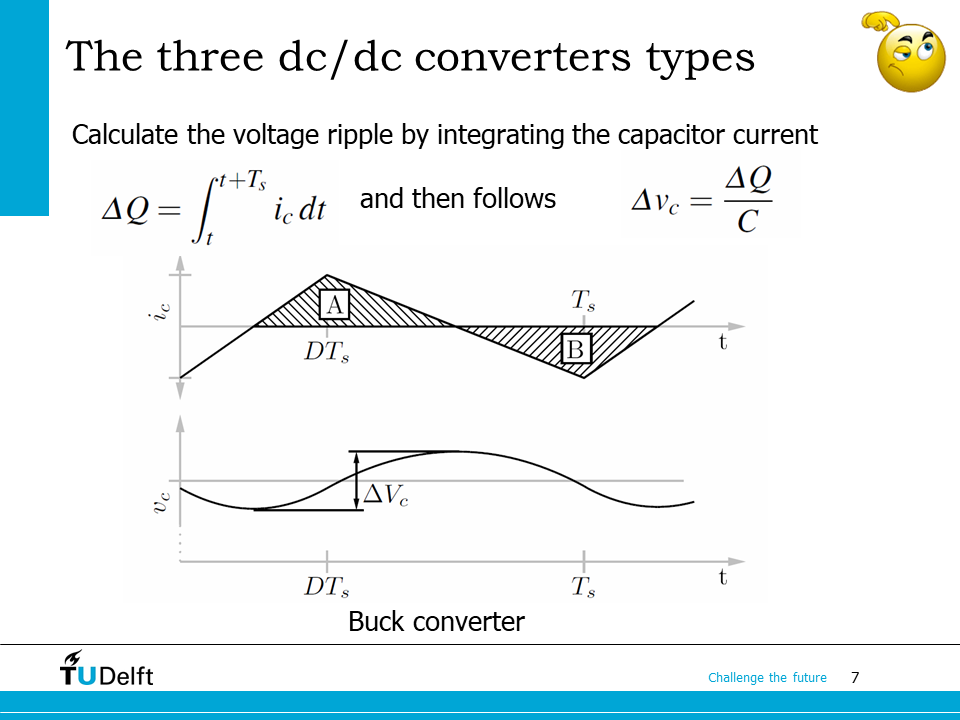
The output voltage ripple can be calculated from the charge going into or leaving out of the capacitor in one switching cycle, which can be solved by integrating the capacitor current.
In the buck converter, the capacitor current has a triangular shape, so \(\Delta Q\) can be solved from the area A or B, which is
The voltage ripple is therefore
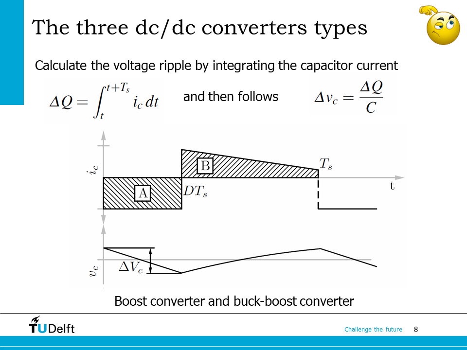
For the boost converter and the buck-boost converter, the capacitor current waveforms are the same, since in both, the capacitor provides the output current when the switch is closed, and gets charged by the difference between the inductor current and the load current when the switch is open.
If the capacitor current does not cross zero when the switch is open, \(\Delta Q\) can be solved as the area of A
Then the voltage ripple is \(\Delta v_c = \Delta Q/C\).
If the capacitor current crosses zero, the equation to calculate \(\Delta Q\) is invalid anymore. Then we have to use the approach presented in Boost Converter. It will not be repeated here.
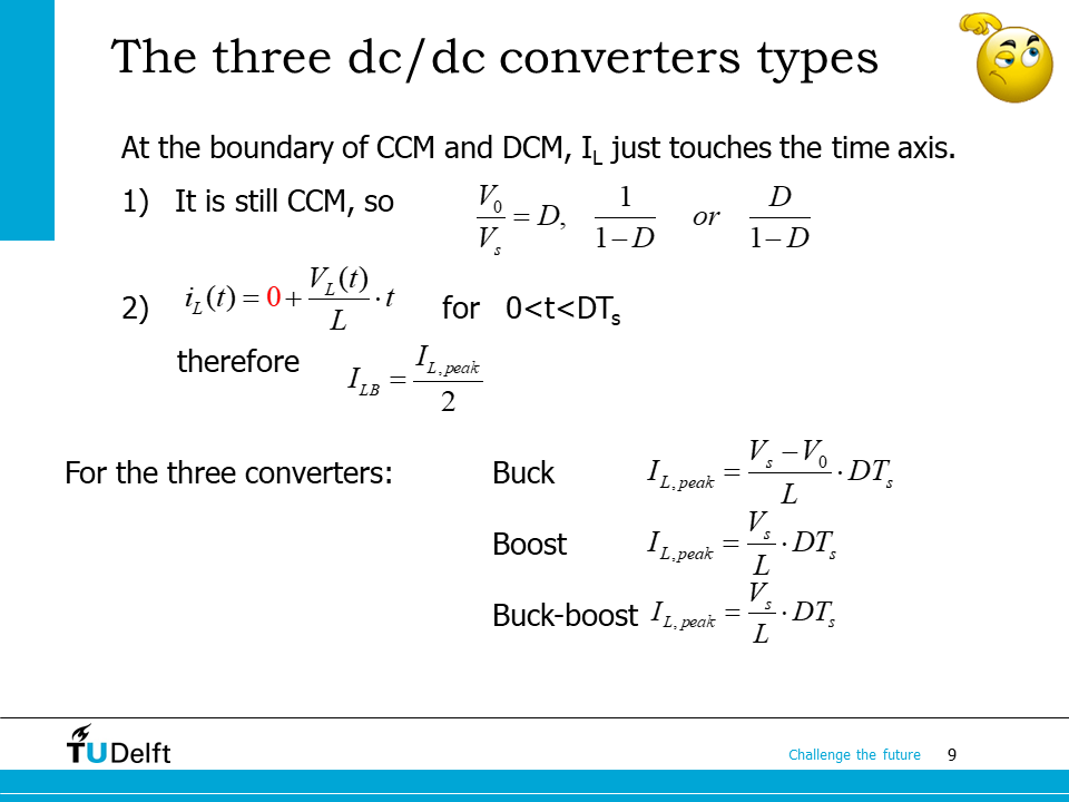
Here it compares the boundary condition inductor current between CCM and DCM for the three topologies. At the boundary, the voltage transfer ratios derived previously are still valide. But the triangular inductor current will reach zero at minimum, so the peak inductor current will be exactly twice of the average inductor current. Based on the current slopes, we can derive, for buck converter, the boundary peak current is
Similarly, for boost converter we have,
For buck-boost converter,
12.1. DC-DC converter exercise#
In the coming slides, we will practice what we have learnt with several exercises.
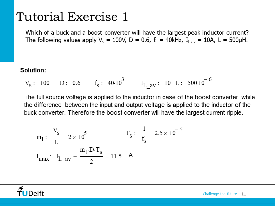
From the first one we can see that if the same input voltage, duty cycle, switching frequency and circuit parameters are used, the boost converter has a higher inductor current ripple since the current slope is steeper.
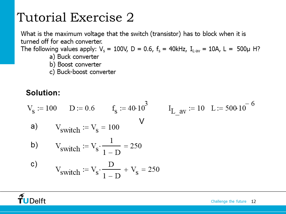
From this exercise, we can see the power semiconductor switch has to block:
the input voltage in a buck converter;
the output voltage in a boost converter;
the sum of the input voltage and the output voltage in a buck-boost converter.
The above conclusions can be drawn from circuit analysis when the switch is off.
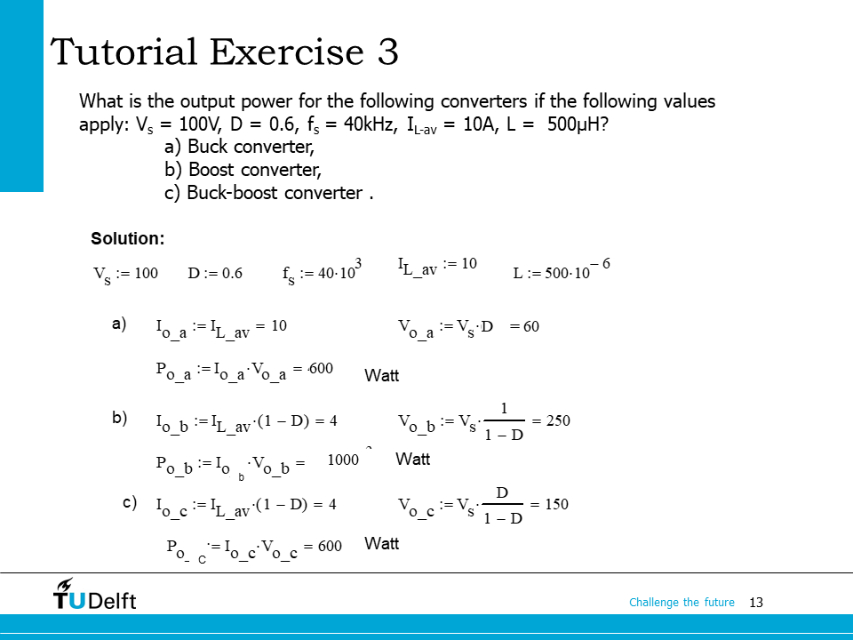
The output power of the three topologies should be solved from the output voltage and the output current. For the buck converter, the output current is the average inductor current, so
For the boost converter, the input current is the average inductor current, so
For the buck-boost converter, the output current is provided by the capacitor when the switch is on, so when \(0\leq t<DT_s\), we have
When \( DT_s \leq t \leq T_s\), the output current is provided by the difference between the inductor current and the capacitor current when the switch is off, so
By integrating the above equations and summing them up, we have
Therefore we have \(I_o = (1-D)I_{L-av}\). Here the steady state assumption is used, so that the accumulated charge (integral of capacitor current) in the capacitor during one switching cycle is zero.
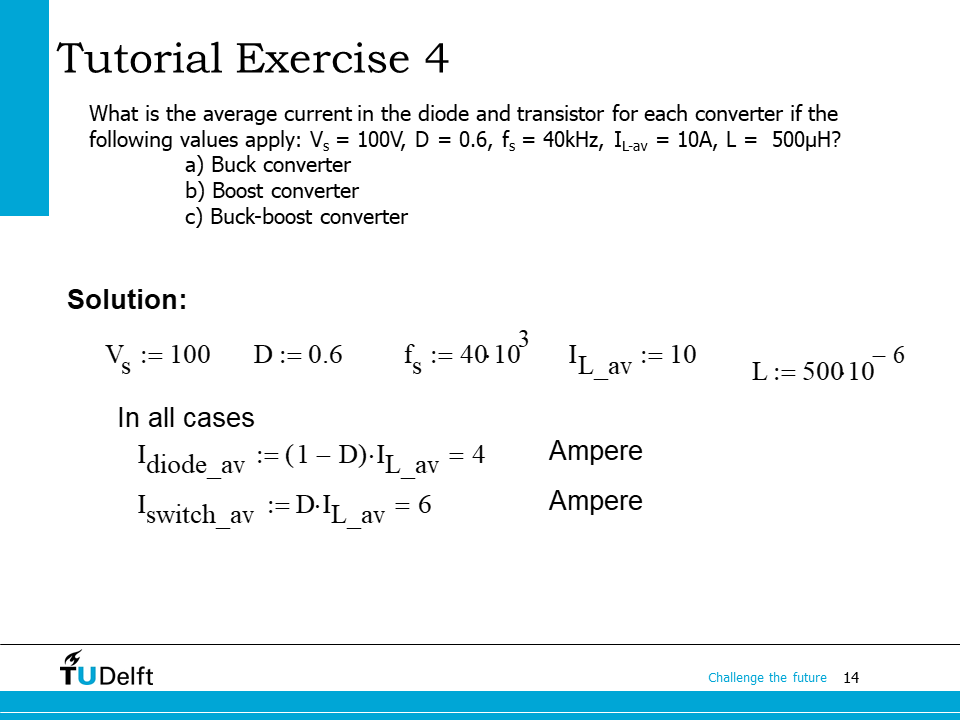
In all three topologies, we can see the switch current is zero when it is open, and takes the inductor current when it is closed, so we have
Similarly, the diode conducts only when the switch is open, so
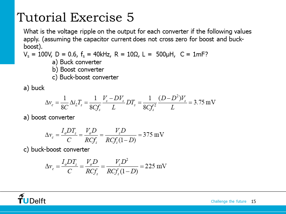
This exercise is to calculate the output voltage ripples. Please first try work it out yourself and click the code below for detailed solution.
Show code cell source
Vs = 100
D  = 0.6
fs = 40.0e3
R  = 10.0
L  = 500e-6
C  = 1e-3
Ts = 1/fs

# buck converter
# dQ = 1/8*diL*Ts, the area of the triangle
Vo = Vs*D
diL = (Vs-Vo)*D*Ts/L
dQ  = 1/8.0*diL*Ts
dVca = dQ/C
print(f'The output voltage ripple of the buck converter is {1000*dVca:.3f} mV.')

# boost converter
# dQ = DTs*Io, since the capacitor current does not go below zero
Vo = Vs/(1-D)
Io = Vo/R
dQ = D*Ts*Io
dVcb = dQ/C
print(f'The output voltage ripple of the boost converter is {1000*dVcb:.3f} mV.')

# buck-boost converter
# dQ = DTs*Io, since the capacitor current does not go below zero
Vo = Vs*D/(1-D)
Io = Vo/R
dQ = D*Ts*Io
dVcb = dQ/C
print(f'The output voltage ripple of the boost converter is {1000*dVcb:.3f} mV.')
The output voltage ripple of the buck converter is 3.750 mV.
The output voltage ripple of the boost converter is 375.000 mV.
The output voltage ripple of the boost converter is 225.000 mV.
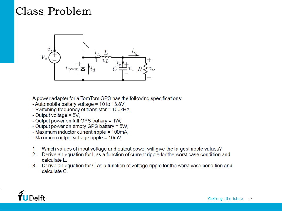
The last problem is reserved as a class problem. Please try to work it out yourself then click the code below for the detailed solution.
Show code cell source
%reset -f
from IPython.display import display, Markdown, Math, Latex

Vbat_min = 10.0
Vbat_max = 13.8
fs       = 100.e3
Vo       = 5.0
Po_min   = 1.0
Po_max   = 5.0
dIL_max  = 0.1
dvc_max  = 0.01

# question 1:
# First the converter is a buck converter.
# The current ripple is below the output current in worst scenario, so it works in CCM.
# We know the inductor current ripple in the buck converter is calculated as (V_s-V_o)/L*D*T_s = (1/D-1)V_o/L*D*T_s = (1-D)V_o/L*T_s
# so the largest inductor current ripple happens when D is minimal, or when the input voltage is the largest
# the output voltage ripple is calculated as 1/8*dIL*Ts/C = 1/8*(1-D)V_o/L*T_s*T_s/C
print('Q1: Both ripple values happen when the input voltage is 13.8 V.')

# question 2:
# dIL = (V_s-V_o)/L*D*T_s = (V_s-V_o)/L*V_o/V_s*T_s
# so the equation is
print('Q2: the equation for L is')
display(Math('$L = {{(V_o-{V_o^2 \over V_s})}\over {f_s\Delta I_{L,max}}}$'))
L = (Vo-Vo**2/Vbat_max)/fs/dIL_max
print(f'L = {L*1000:.3f} mH.')

# question 3:
# dvc_max = 1/8*(1-V_o/V_s)V_o/L*T_s*T_s/C
# so the equation is
print('Q2: the equation for C is')
display(Math('$C = {{1 \over 8}{(V_o-{V_o^2 \over V_s})}\over {f_s^2 L \Delta v_{C,max}}}$'))
C = 1/8*(Vo-Vo**2/Vbat_max)/L/fs/fs/dvc_max
print(f'C = {C*1000000:.3f} uF.')
Q1: Both ripple values happen when the input voltage is 13.8 V.
Q2: the equation for L is
L = 0.319 mH.
Q2: the equation for C is
C = 12.500 uF.