6. Power Electronics Basics: Linear and Switchmode Voltage Regulator#
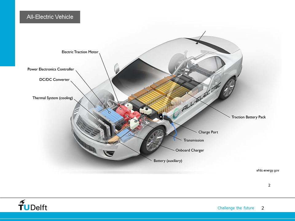
Welcome to the first lecture of the power electronics module of this course. We use the EV as an example again to explain the role power electronics plays in practice. As you can see, inside the EV, there is an on board chargers to charge the batteries, a DC/DC converter to transform the low voltage of the battery to the high voltage required by the electric traction motor drive, the inverter to drive the traction motor and some auxiliary power supplies etc. All those components are enabled by power electronics technologies.
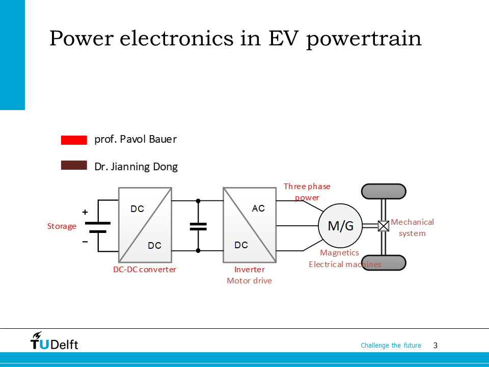
In the coming lectures of this module, we will focus particularly on DC-DC converters and DC/AC converters (inverter). The latter one will be addressed further in the AC motor drive part of the course.
The content of this lecture is listed here. We will start from linear voltage regulator, which is an outdated technology, then move to the transistor based linear voltage regulator. After that, we will briefly discuss the switching-mode operation of transistors and how to use it for voltage regulation, which forms the base for power electronics.
After taking the lecture, we are supposed to master the objectives listed here. We should be able to tell the working principles of a linear regulator and a switched regulator, and understand the differences between them. More importantly, we should be able to tell how pulse width modulation works in power electronics after taking the lecture.
6.1. Linear voltage regulator#
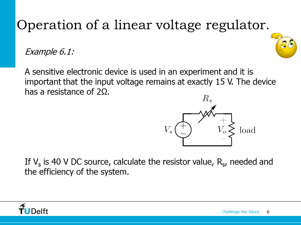
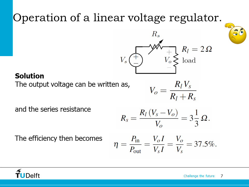
A linear voltage regulator is shown on the slide. It composes of a variable resistor \(R_s\), a DC source \(V_s\), and a load with a resistance of \(2~\Omega\). In order to keep the load at exactly \(15~\mathrm{V}\), we have to solve for \(R_s\) by applying the Kirchhoff’s voltage law. The efficiency can then be solved from the load resistance to the total resistance ratio since they share the same current.
The solution can be found by clicking the block below.
Click here for the solution.
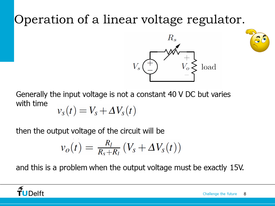
So in general, we will apply this type of voltage regulator to a sensitive load, it becomes problematic because the circuit is not able to handle the fluctuation in the input voltage, as shown in the derivation here.
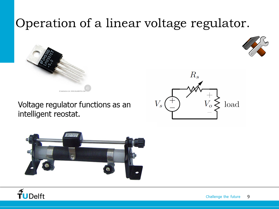
In practice, we often use linear voltage regulator chips like the one shown on the top left of the slide. It functions as an intelligent rheostat, which changes its resistance \(R_s\) according to the load and the input voltage, so that a stable output \(V_o\) is obtained.
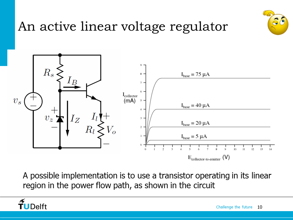
A possible implementation of the aforementioned linear regulator with stable output voltage is to add a transistor and a Zener diode in the circuit to form an active linear voltage regulator. We know for the Zener diode, when it is reverse-biased, the voltage across it will change very little for large current changes in the diode, and for a transistor, the emitter current can be controlled by the relatively small base current when it is operating in the linear mode.
As shown in the circuit, the input voltage is time-varying:
When the nominal supply voltage \(V_s\) is sufficiently greater than the Zener voltage \(V_Z\), the transistor will be in the linear region, such that the base-emitter voltage \(v_{be}\) is approximately the base-emitter junction offset voltage \(V_\gamma\). The output voltage is therefore:
which is constant. As we can see, by adding the Zener diode and the transistor, the output voltage becomes relatively independent of fluctuations in the unregulated source voltage and the required load current. This technology to regulate voltage used to be often used to build power supplied. However, there is still substantial loss in the resistor, and requires large heatsink to cool the components. A modern equivalent based on the state-of-the-art power electronics technologies can be much lighter and more efficient.
6.2. Operation of transistors#
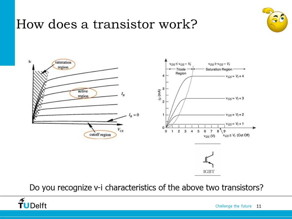
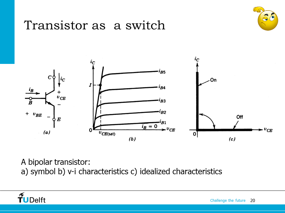
It requires the understanding of the operation of the bipolar junction transistor to do the analysis above, which is covered in the course EE1C31. Here you can see two types of transistors: on the left, what you see is a bipolar transistor, whose collector current \(i_C\) is directly proportional to its base current \(i_B\) over a wide range of collector-to-emitter voltages \(v_{CE}\) in the active region. In the previous example, we let it work in the linear region in the middle (active region). As you can see in this region, the transistor becomes neither fully on nor fully off. A large collector current \(i_C\) will flow through a large collector to emitter voltage \(v_{CE}\). This creates substantial loss in the transistor, which is one of the reasons why the linear voltage regulator requires large heat sink and has lower efficiency.
In modern switched mode power supplies, we either use high \(i_B\) to fully turn on the transistor, so that \(v_{CE}\) is very low (saturation region); or use a zero \(i_B\) to completely turn off the transistor (cutoff region). In this way we are able to do the power conversion without wasting a lot of power in the transistor (\(v_{CE}*i_{C}\). Therefore, a bipolar junction temperature is also called a current controlled device. The major drawback of such device in switching power supply is they are relatively slow in changing from the on to the off state and vice versa, since a relatively large base current has to be applied or removed when they are turned on or off.
On the right hand side, what you see is the characteristics of a voltage controlled device. It is called insulated-gate bipolar transistor (IGBT). It is similar to the power transistor, except that it is controlled by the voltage applied to a gate rather than the current flowing into the base as in the power transistor. The impedance of the control gate is very high in an IGBT, so the amount of current flowing in the gate is extremely small. It is a essentially a hybrid device which combines features of both metal-oxide-semiconductor field-effect transistor (MOSFET) and a bipolar junction transistor. The circuit symols of the IGBT is shown below the characteristics plot. Since it is controlled by a gate voltage with very little current flow, the IGBT can be switched more rapidly than a conventional bipolar junction transistor.
In modern power electronics, MOSFETs are also often used as power switches. It can be operated as a switch by applying different gate voltages to drive it change between ohmic state and the cut-off state.
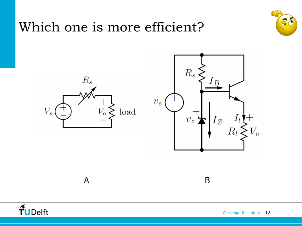
Now let’s check the question on the slide. Apparently, because the loss in the transistor, circuit A is more efficiency than circuit B.
6.3. Overview of power converters#
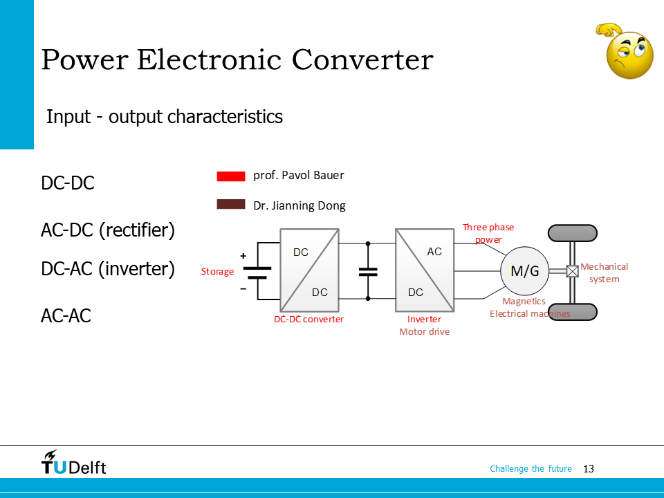
Previous example shows a converter which transforms one DC voltage level to another DC voltage level, which is called a DC-DC converter. Depending on the input-output characteristics, there are also AC-DC converters, which are also called rectifiers, DC-AC converters (inverter) and AC-AC converters. They have different applications in practice. For example, inverter can be used to drive an AC motor from DC source or for grid interfacing of solar panels, rectifier can be used for charging of batteries from AC grid.
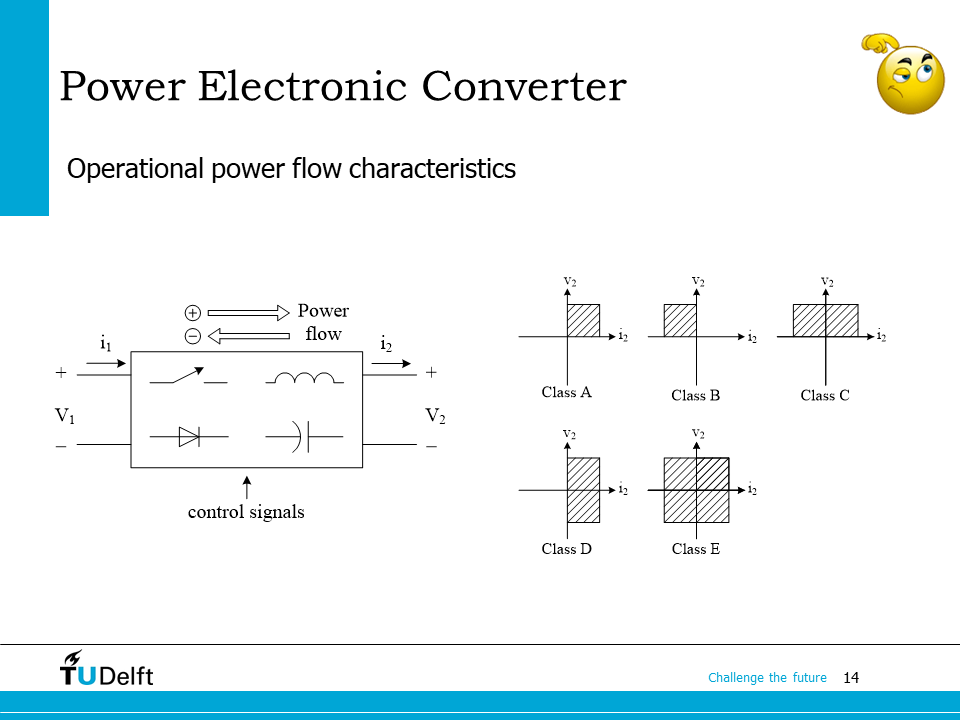
Based on the power flow direction, we are able to divide power converters into several classes. As we can see on the slide, the coordinate system formed by output voltage \(v_2\) and current \(i_2\) can divide the domain into four quadrants by the signs of them.
In class A converter, both output voltage and positive, so power flows from input to output and is uni-directional. Similarly, power flow is class B is uni-directional as well, but is from output to input. These two types of converters are also called one-quadrant power converters.
For class C and D, either current or voltage can change its sign but not both, so power flow is able to flow back and forth (bi-directional) by changing either one of them. These two types are also called two-quadrant power converters.
The class E converter is able to deliver both positive/negative voltage and current, so the power is bi-direction disregarding the sign of \(v_2\) or \(i_2\). The converter works in all four quadrant. Thus it is also called a four-quadrant converter.
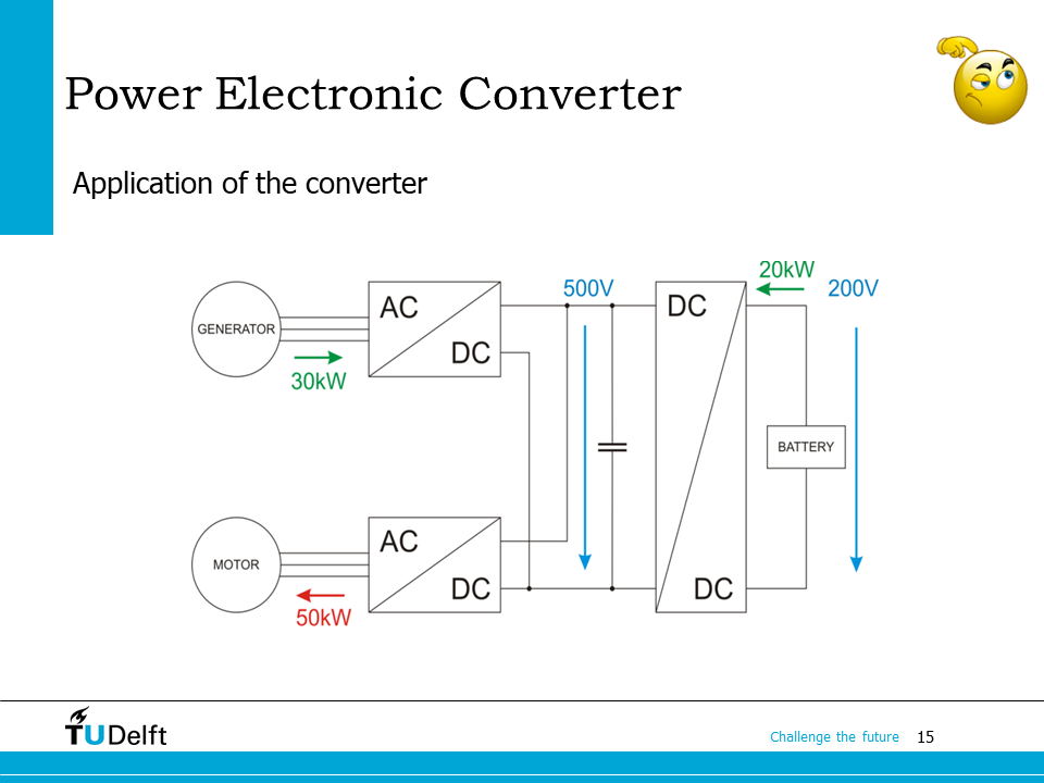
By combing different types of converters, we will be able to transform between AC and DC, and also control the direction of power flow to form a more complicated system to meet our purpose. For example, here it shows a system to power a motor from both a generator and a battery. By controlling the power converters, when the generator is generating excess power more than the motor can take, it can be routed to the battery. Otherwise, when the motor requires more power than the generator can deliver, the battery can release the energy stored via the DC-DC converter. In this applications, the DC-DC converter should be a two-quadrant converter since we need bi-directional power flow.
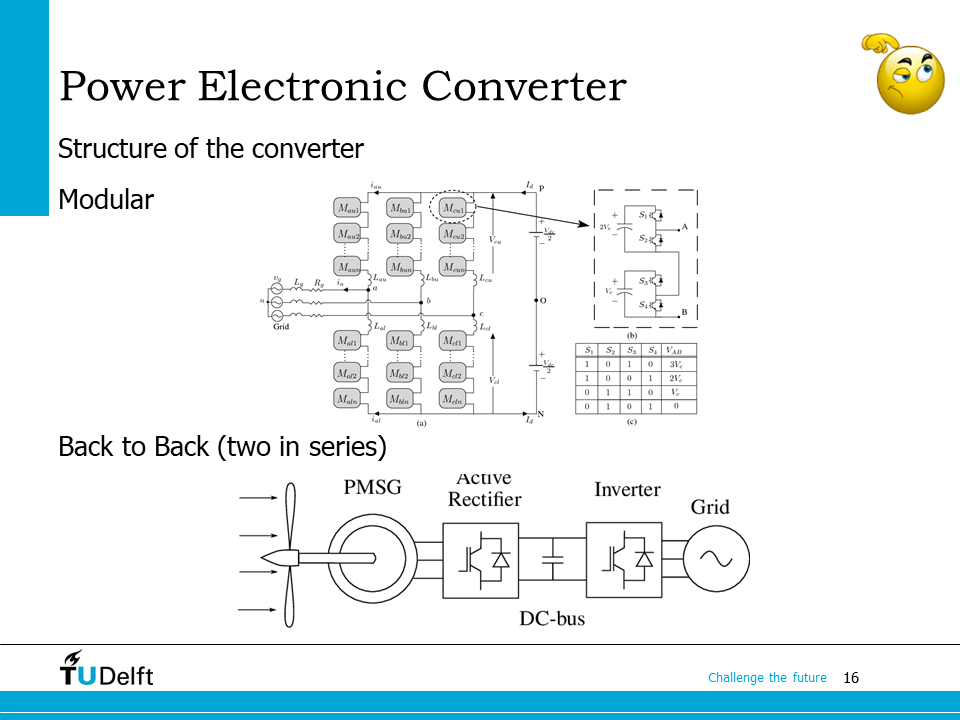
There are multiple ways to construct a power converter. Here it shows two commonly used structure. On top, it shows a multi-level modular converter (MMC) where many modules with the same topology are used to form a large inverter which is able to handle high voltage and large power.
On the bottom, it shows a series structure, where an active rectifier is connected to an inverter at the same DC bus to from a back to back system, so that we will be able to convert variable frequency AC power from the wind generator to fixed frequency AC power required by the grid.
6.4. Regulator with switching transistors#
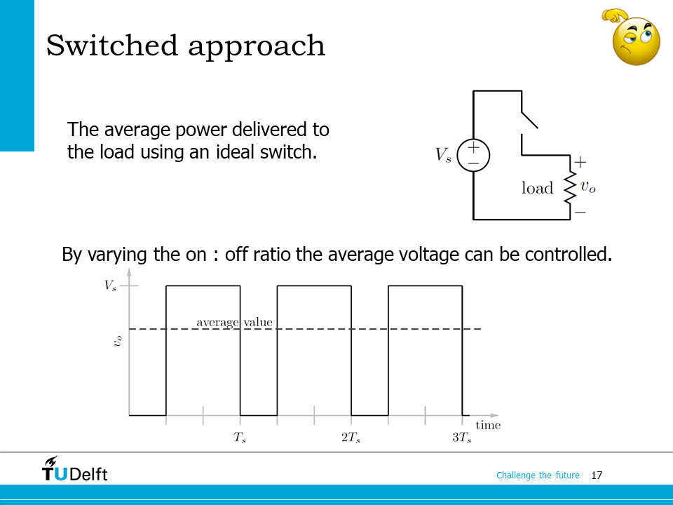
We previously mentioned a more efficient way to use transistors for power conversion is to use them in the switched mode. On this slide, it shows a power source \(V_s\) is supplying the load \(v_o\) via an ideal switch, i.e., the switch can easily be switched on or off and that it does not produce any additional loss.
It is straightforward to imagine that if we need \(v_o\) to be \(V_s\), we only need to keep the switch always on. If we need a zero output voltage, we can simply turn off the switch all the time. To obtain any voltage in between, we have to vary the on time to off time ratio so that the average voltage meet what is required.
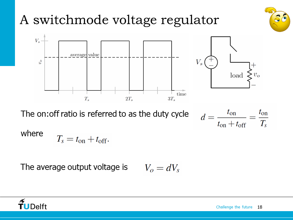
As we can see on the slide, the switch is switched on and off with a time cycle (switching period) of \(T_s\). In each switching period, the on time to period ratio is defined as the duty cycle, or denoted by the symbol \(d\), therefore, we will be able to solve the time average output voltage as
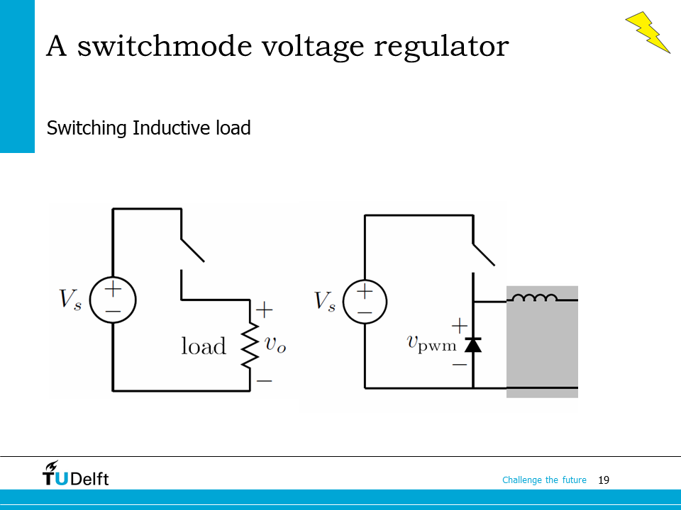
The previously discussed switched voltage regulator works well for a resistive load, however, it creates a problem if the load is inductive. If the current in an inductor is suddenly turned off, there will be an infinitely high voltage induced as \(L\mathrm{d} i/ \mathrm{d}t\). In order to avoid over voltage, we have to provide a path for the current to continue flowing when the switch is turned off. The solution is to put a diode in parallel to the load.
As we can see in the figure on the right hand side, the diode is reverse-biased when the switch is on, the current flows from the source to the load via the switch. When the switch is turned off, the load current can continue flowing via the diode since it is now forward-biased, and there will be only a small junction voltage drop on the diode.
In practice, the ideal switches should be implemented by power semiconductor devices working in the switched mode. Here it shows the symbol and the characteristics of the power bipolar junction transistor, which has been addressed in the last section.
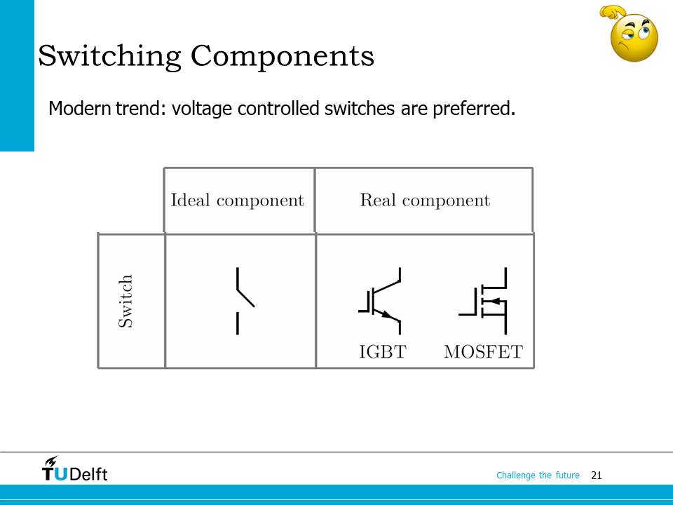
In modern applications, voltage controlled devices are preferred because they are more rapid in switching and more efficient. In practice, we often use IGBT or MOSFET to realise the switching. Both of them can be treated as ideal switches in this course, since we are not considering the non-ideal characteristics of them. Since we are able to control their on/off states by gate signals, they are also called “controlled switches”. We will come back to the assumptions and their limits of “ideal components” later.
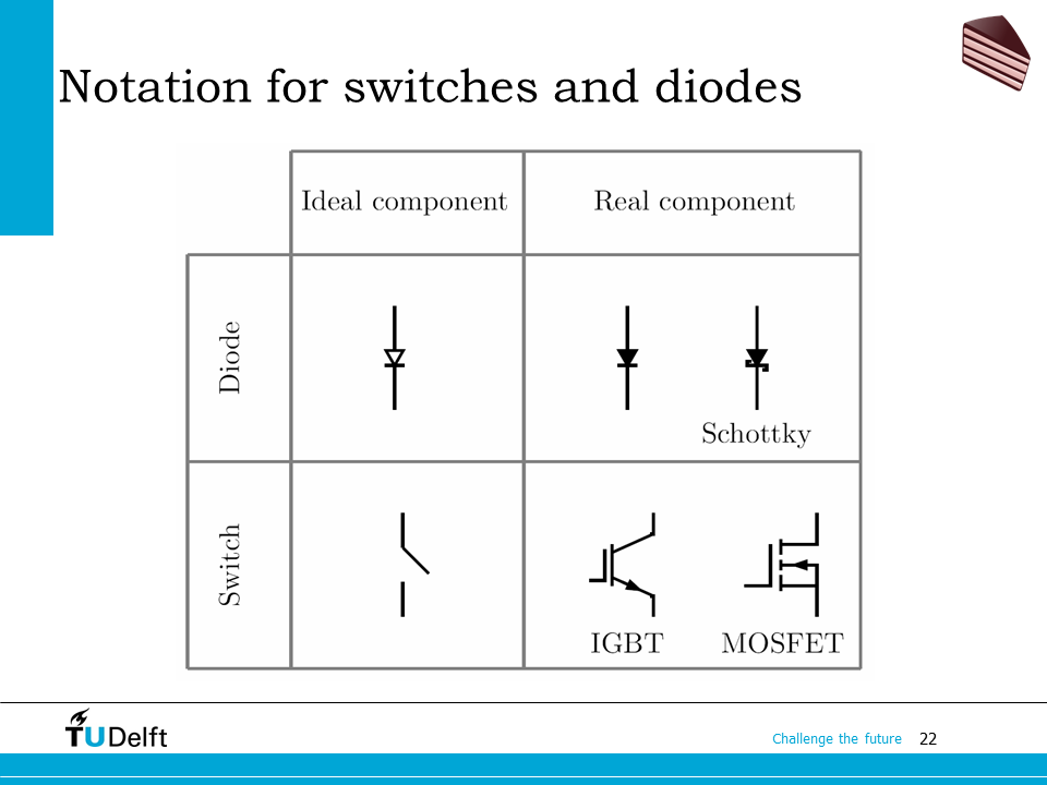
Similarly, for the diode, we also assume it is ideal in the analysis for the rest of the course. We could consider it as “uncontrolled switch” will be turned on or off by the voltage across it. By treating it as ideal component, we assume it is able to block any reverse-biased voltage and can be treated as short-circuit when it is forward-biased.
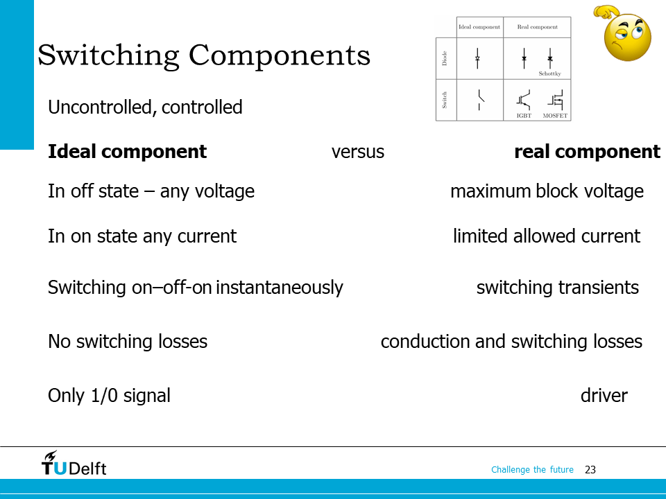
Hereby we summarise all the assumptions we make for the ideal components and their limits when compared to real components, for both uncontrolled and controlled devices.
For all switches we will assume that:
When in the off-state the switch can handle any voltage across it and will not fail.
When in the on-state the switch can handle any current through it without failing.
The switch can switch instantaneously from the off-state to the on-state and vice versa.
There are no losses associated with the switching cycle.
The switch only requires a signal to control the state of the switch. We will assume that if the control signal is equal to “1” the switch will be closed (i.e. in the on-state) and when the signal is equal to “0” the switch is in the off-state.
But in real components, the block voltage at off-sate and the current at on-state are both limited. The real switches are not able to be turned on/off instantaneously, and there is always switching transients. There are also conduction loss and switching loss when a real component is in operation. Moreover, to drive a real controlled component, we have to implement a gate driver circuit, which is much more complicated than only 1/0 signals.
Although the behaviours of real components are outside of the scope of this course, we should be aware that the analysis we’ve learnt in this course has its limitations since above mentioned non-ideal behaviours are not considered.
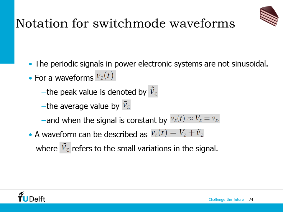
Before we move further to analyse various kinds of switched power converters, we should set the notation we use for switched-mode waveforms. For a switched-mode waveform \(v_z(t)\), its peak value can be represented as the hatted symbol \(\hat{v}_z\). Similarly the average value is represented by its barred version \(\bar{v}_z\) or the capital version \(V_z\).
Then \(v_z(t)\) would be able to be described as the average value \(V_z\) plus its ripple \(\tilde{v}_z\). The ripple waveform \(\tilde{v}_z\) represents the small variations in the signal.
6.5. Pulse width modulation#
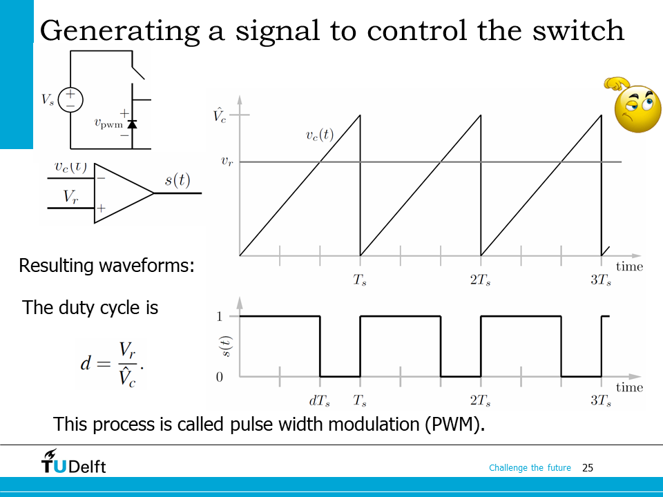
There is still one question to be answered for the switched power converter: how to generate a proper switching signal so that the converter gives us the requested voltage. This is usually solved by the pulse-width-modulation (PWM) technique. A sawtooth or triangular wave \(v_c(t)\) is used as the so called carrier wave. Then a reference voltage \(V_r\) is compared with the carrier wave via a comparator. The output from the comparator will be used as the switching signal.
When \(V_r\) is higher than \(v_c(t)\), \(s(t)\) gives a “1” signal to turn on the switch, otherwise a “0” signal is produced to turn off the switch. Therefore, the duty cycle is the ratio between the reference voltage and the peak of the carrier wave \(\hat{V}_c\).
In this way, we would be able to control the output voltage with a reference voltage proportional to it.