13. Flyback Converter#
In the previous lectures of the module, the topologies we studied are all non-isolated dc/dc converters, which means the input and ouput are not galvanically isolated.
Here we introduce the concept of galvanic isolation. It means that we electrically isolate different sections of an electrical systems to prevent current flowing between the sections. No direct conduction path is permitted in galvanic isolation, so the energy exchange between the sections should be done by other means, such as capacitance, induction or electromagnetic waves. Galvanic isolation is often used to break ground loops to prevent accidental current from flowing to ground through a person’s body.
In this lecture, we will take a dip into the isolated dc/dc converter, and study one of the most commonly used topology for isolated DC/DC converter: flyback.
After taking this lecture, we should be able to understand what galvanic isolation is and its advantages. Then we should be able to tell the working principle of a coupled inductor and the benefits of it. In the end, we should be able to understand and calculate the performance of a flyback converter.
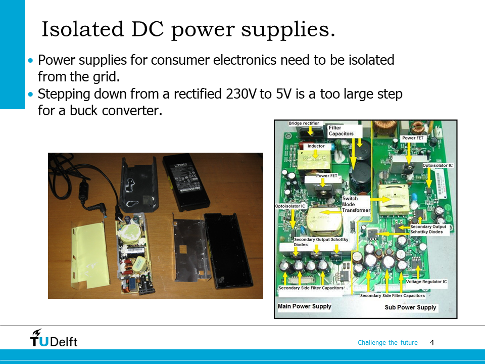
Consumer electronics, including computers and home appliances, should be touched by the user when it is in operation. It is critical to make sure there is no current path from the grid to the ground through the person using them. That is why galvanic isolation is essential in those products.
Another advantage of having galvanic isolation is that we are able to reach large voltage transfer ratio via coupled inductor, as we will see later. In many consumer products, voltage as low as 5 V is needed. To convert the rectified 230 V to such low voltage via a buck converter, the duty cycle would be very low. A low duty cycle will increase the loss of the buck converter because of the long conduction time of the diode. By using a coupled inductor, or an isolation transformer, the voltage transfer ratio can be realised by the turns ratio, while the duty cycle of the switch can be maintained in a reasonable range.
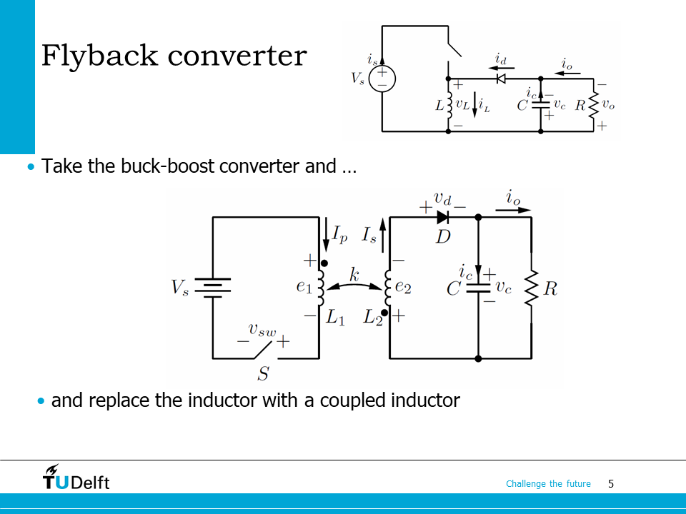
A flyback converter realizes the aforementioned large voltage transfer ratio via a coupled inductor. As shown on the slide, the flyback converter is derived from the buck-boost converter by replacing the buck-boost converter’s inductor with a coupled inductor.
The coupled inductor can be viewed as two inductors sharing a common core with opposite polarity windings, as indicated by the dot notation in the schematic.
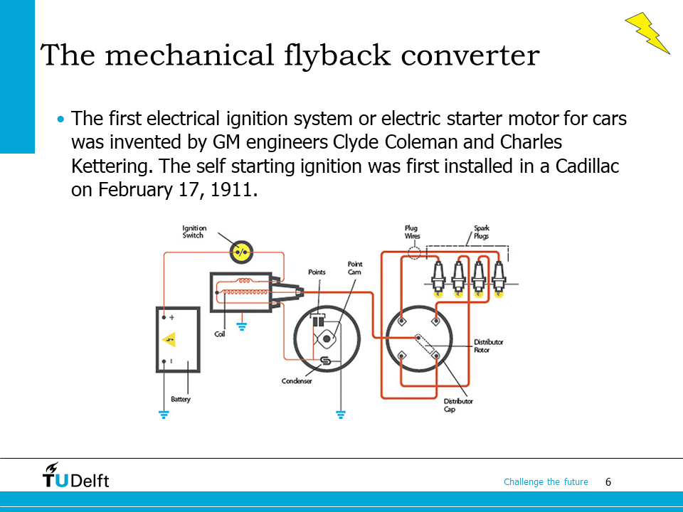
Actually the concept of flyback was invented before power semiconductors. As can be seen on the slide, a flyback converter is used in the electrical ignition system. The coil shown on the slide has two windings wounded on the same core. The number of turns of the secondary coil (ignition coil) is far larger than that of the primary coil. When the ignition switch is on, the primary coil is turned on and off by the rotating point cam. When the primary coil is on, electrical energy is stored in the magnetic field. When the primary coil is turned off by the point cam, the stored magnetic field collapses, and energy is released through the ignition coil, which has a large number of turns, to the electrodes of the spark plug via the distributor. Because of the large number of turns, the ignition coil is able to convert a 6 or 12 V of a battery into a very high voltage of about 15000 to 30000 V between the electrodes of the spark plug, which is high enough to generate sparks for ignition.
A modern flyback converter works in the same way. The only difference is that we will replace the mechanical switch based on the point cam with power semiconductor switches.
To analyze the flyback converter in detail, we first have to study the coupled inductor, which we have learnt in the course EE1C21 and will be elaborated in Magnetic Circuit Princiles.
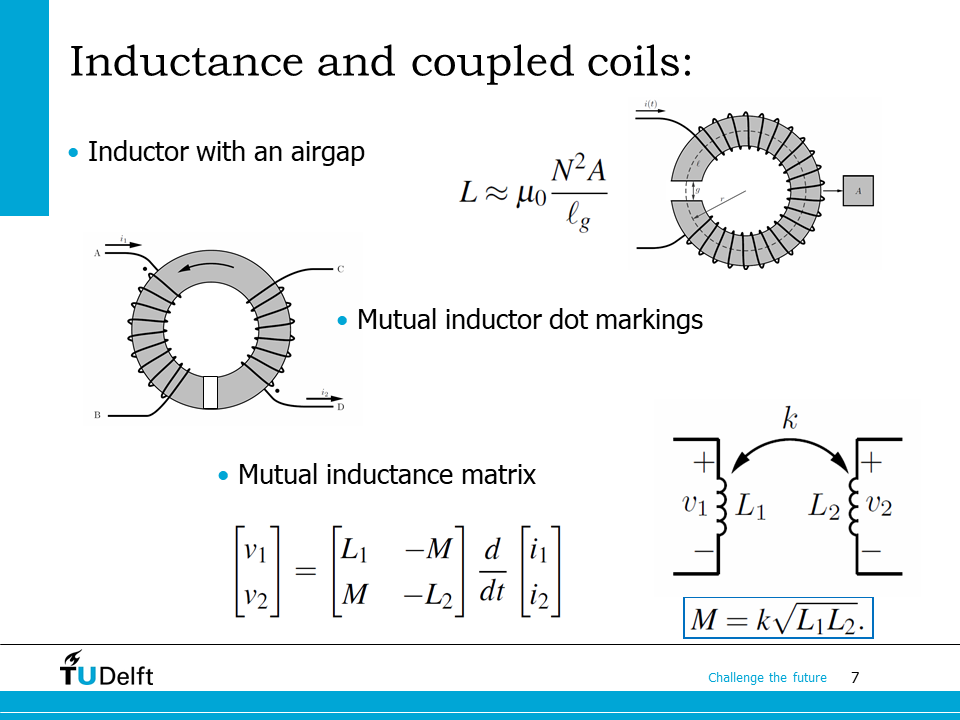
Let’s start with an inductor with a single winding and a magnetic core with air gap. The permeability of the magnetic core material is usually several orders of magnitude higher than that of the air gap, so the inductance will be largerly determined by the air gap.
where \(\mu_0\) is the permeability of air, \(N\) is the number of turns, \(A\) is the cross sectional area of the air gap and \(l_g\) is the length of the air gap. We will see in Magnetic Circuit Principles that this equation is obtained based on several assumptions, which will not be alaborated here.
If we wound a second coil to the magnetic core, the inductor becomes a coupled inductor, where the two coils are coupled to each other through the same magnetic core. Here we can use the dot convention to mark the polarity of the two coils:
Dot convention
When the reference direction of a current enters the dotted terminal of a coil, the reference polarity of the voltage that it induces on the other coil is positive at the dotted terminal. We can also state it differently. When the current enters a coil at the dotted terminal then the current flow due to the induced voltage on the other coil will leave the coil at its dotted terminal.
If the self inductances of the two coils are \(L_1\) and \(L_2\) respectively, the coupling factor between them is \(k\), the mutual inductance would be
Based on the knowledge we learn from EE1C21, we have the mutual inductance matrix
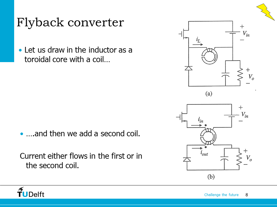
This slide shows how a flyback converter is obtained from a buck-boost converter. As we can see, when the semiconductor switch is turned on, current in the primary coil increases, and energy is stored in the magnetic field, which is \(E = \frac{1}{2}Li_{in}^2\). The diode on the secondary side is reverse biased, so \(i_{out}=0\).
When the semiconductor is turned off, the primary current \(i_{in}\) becomes zero, the magnetic field collapses, the store energy in the magnetic field has to be released via the secondary coil. The secondary diode is forward biased. \(i_{out}\) becomes nonzero, and then decays as the inductor discharges.
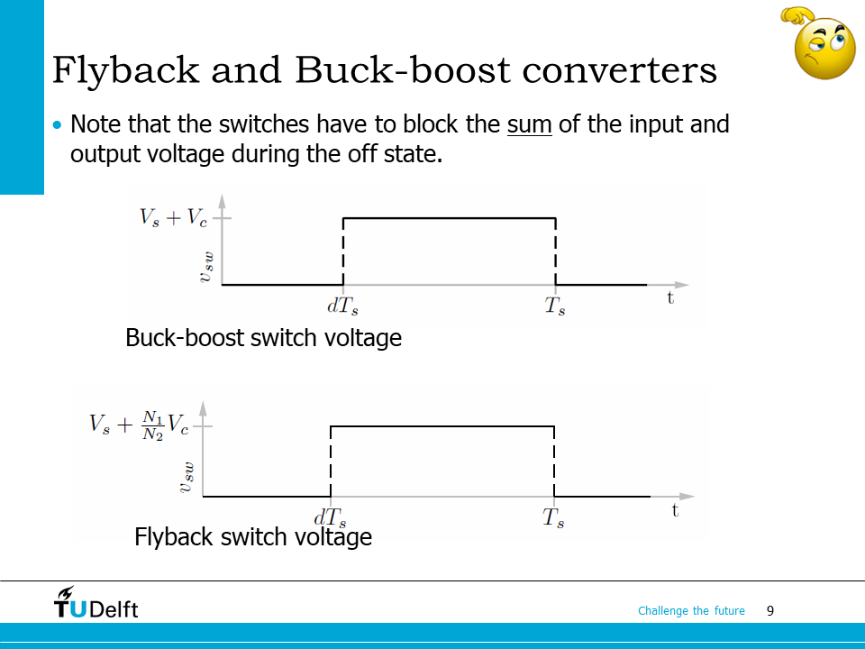
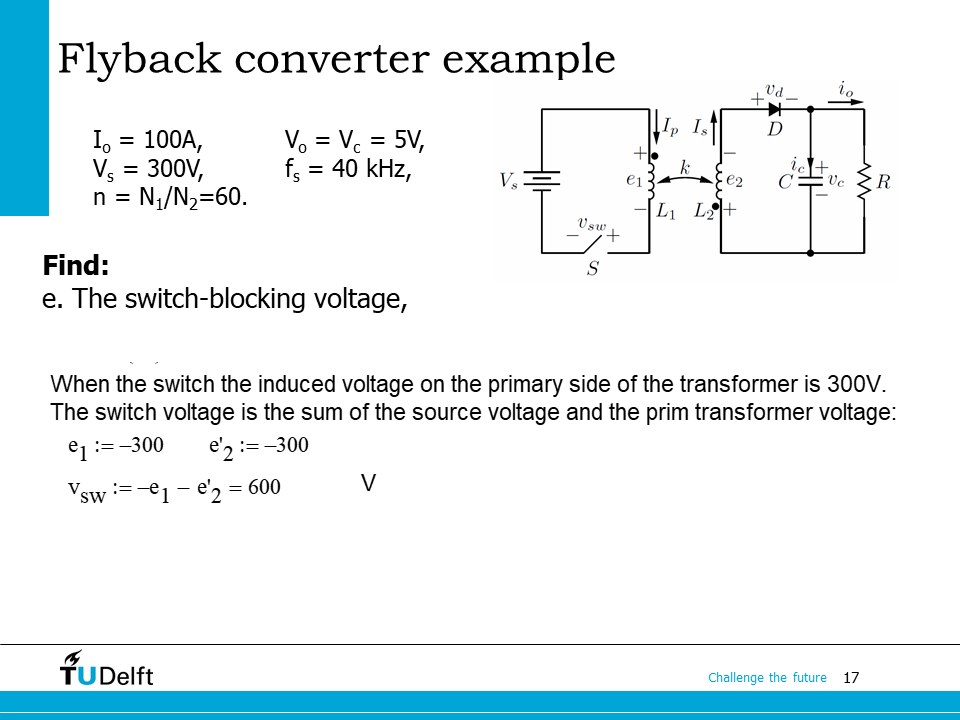
For the original buck-boost converter, during the off state, the switch blocks the sum of the input voltage and the output voltage, as we have learnt in Buck-Boost Converter.
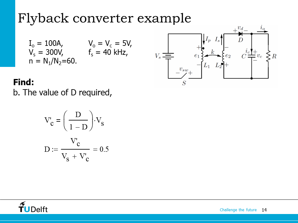
Similarly, for the flyback converter, during the off state, the switch has to block the sum of the input voltage, and the induced voltage from the output voltage, which is calculated from the turns ratio of the coupled inductor \(N_1/N_2\):
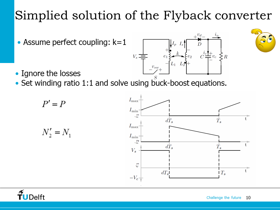
If we assume a perfect coupling, i.e. \(k = 1\), or there is no leakage in the coupled inductor, the flyback converter can be simplified as the schematic shown on top right of the slide, where we have the induced voltage ratio the same as the turns ratio:
By further assuming there is no loss in the coupled inductor, and referring the secondary parameters to the primary side, we would be able to combine the two induced voltages \(e_1\) and \(e_2\) into one, and simplify the converter to a buck-boost converter.
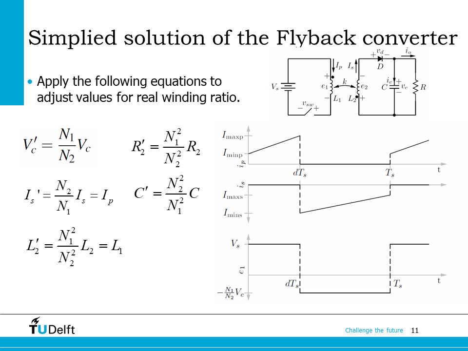
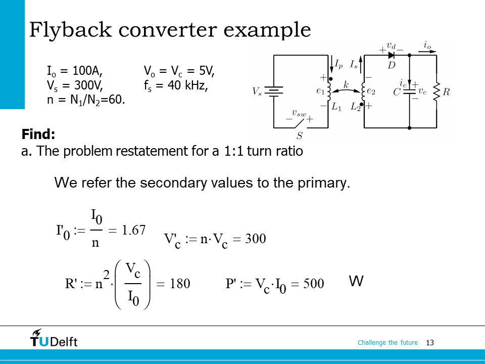
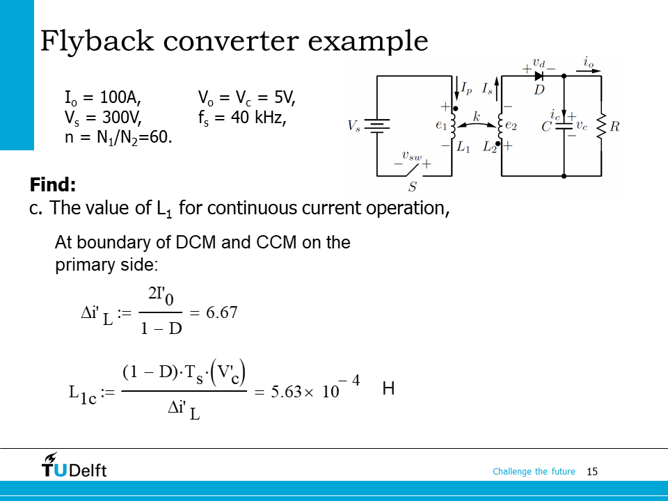
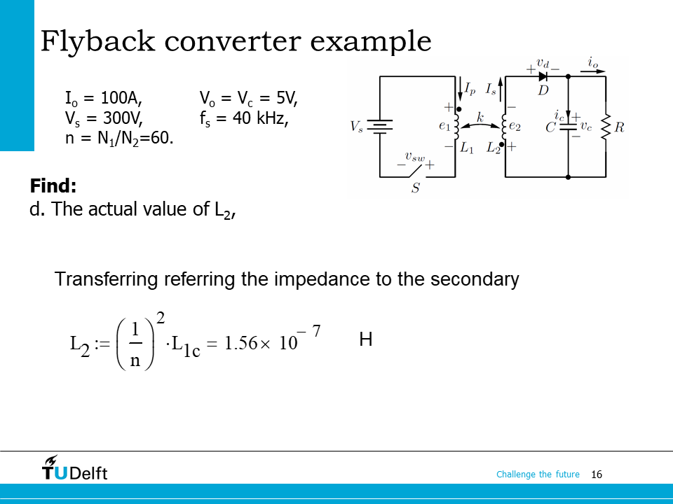
Based on the approach described previously, to deal with a flyback converter with an arbitrary turns ratio \(N_1:N_2\), the secondary voltage, current and impedance should be referred to the primary side, so that we are able to analyse it as a buck-boost converter.
The primed symbols in the equations below represent the values referred to the primary side.
Attention
When referring the capacitance to the secondary side to the primary side, the transfer ratio is \(N_2^2/N_1^2\), which is the inverse of that for the inductance and the resistance. Please think about this and try to give the explanation.
After referring all the secondary quantities to the primary side, we will be able to solve the flyback problem as a buck-boost converter, then transfer the referred quantities back to the secondary side.
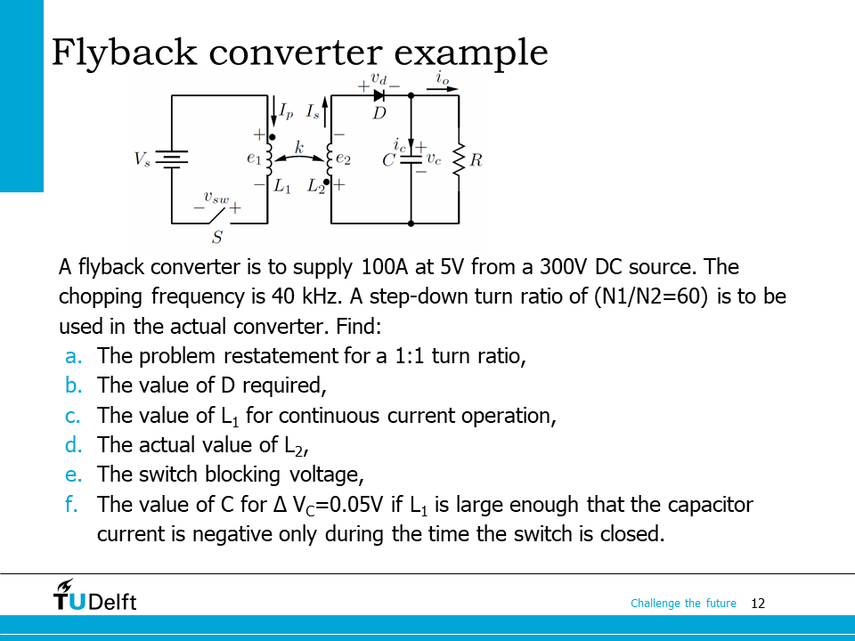
Let us take this problem as an example to show how the approach described above is applied to a flyback converter.
Please first try to solve it yourself then click the block below for the solution. A piece of Python code is also available to show the detailed calculation procedure.
Click here for solution.
Show code cell source
Vc = 5.0
Is = 100.0
Vp = 300.0
fs = 40.0e3
N1_to_N2 = 60.0
dVc = 0.05
# question a problem restatement
# refer all secondary quantities to the primary side
Vc_p = Vc*N1_to_N2
Is_p = Is/N1_to_N2
print(f'a. the problem restatement is: a buck-boost converter is to supply {Is_p:.3f} A at {Vc_p:.3f} V from a 300V DC source. The chopping frequency is 40 kHz.')
# b. for the restated buck-boost converter: D/(1-D) = Vc/Vs, so
D = 1/(1+Vp/Vc_p)
print(f'b. the required duty cycle D is {D}.')
# c. boundary condition inductance: happens when dIL = 2*ILav
# ILav*(1-D) = Is'
# dIL = Vp/L*D*Ts
# so we have:
ILav = Is_p/(1-D)
LB = Vp*D/fs/(2*ILav)
print(f'c. To maintain CCM, inductance L1 should meet L1 >= {LB*1e6} uH.')
# d. actual value of L2 is obtained from turns ratio
L2 = LB/(N1_to_N2)**2
print(f'd. Actual value of L2 is {L2*1e6} uH.')
# e. switching block voltage
# it should block the primary input voltage + the induced voltage on the primary coil from the secondary side
# so we have
Vsw = Vp+Vc_p
print(f'e. The voltage the switch has to block is {Vsw} V.')
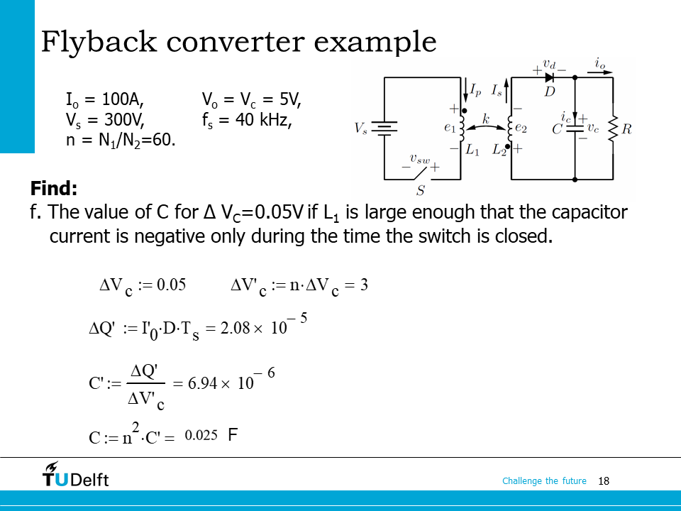
# f. voltage ripple
# first we have to refer the voltage ripple to the primary side, so we can analyze it as a buck-boost
dVc_p = dVc*N1_to_N2
# calculate the charge exchange
dQ_p = D*Is_p/fs
# capacitance referred to the primary side
C_p = dQ_p/dVc_p
# actual capacitance on the secondary side
C = C_p*N1_to_N2**2 # inverse to the inductance ratio
print(f'f. Output capacitance value of L2 is {C*1e3} mF.')
a. the problem restatement is: a buck-boost converter is to supply 1.667 A at 300.000 V from a 300V DC source. The chopping frequency is 40 kHz.
b. the required duty cycle D is 0.5.
c. To maintain CCM, inductance L1 should meet L1 >= 562.5 uH.
d. Actual value of L2 is 0.15625 uH.
e. The voltage the switch has to block is 600.0 V.
f. Output capacitance value of L2 is 24.999999999999996 mF.