Module 1 Online Practical Manual: Contactless Power Transfer#
Introduction#
In this module you are going to investigate and test a contactless transferring power. The system implementation can be approached in a couple of steps.
The steps to design the complete system are:
Design the DC/AC-inverter
Design the AC/DC-rectifier
Design and test an air-core transformer.
Investigate the possibility of transmitting power with the air core transformer.
Learn how to compensate the leakage inductances of the air core transformer to enable it to transmit a considerable amount of power.
Test and evaluate the complete power transfer system and measure the efficiency.
The steps are split in several assignments. The inverter and rectifier you must design by yourself and show the design as schematics presented in the practical report. In assignment 1 several parts of the inverter are explained. Alternatively you can read extra literature (e.g. papers, books, etc.).
The deliverable will be a practical report as per requirements given in each assignment.
To help you with questions and technical difficulties, a help desk is available. Please contact Joris Koeners via email if you have any questions and if needed a skype session can be planned.
Assignment 1: design of a contactless power transfer system#
Before doing assignment 1, please read
Read the Power Electronics and the Mangetics parts of the reader;
Datasheets of UC3525 controller IC, IRS2001PBF driver IC, the different switches and diodes (available on Brightspace);
The overcurrent protection subcircuit (available on Brightspace);
Theoretical background section of this manual.
for background knowledge to carry out this assignment.
In assignment 1, you design the converters for a contactless power transfer system by choosing corresponding components from the datasheets available on Brightspace. The design should include:
An Inverter and corresponding gate drivers;
PWM generation and control circuits;
and a rectifier.
The assignment will be filled in section 1 of the practical report of module 1. Please include the following content in section 1 of the report:
A circuit schematic of your designed system showing the components you choose and their interconnections;
Justifications on why you choose specific components (switches and diodes).
Assignment 2: measurements on an inverter feeding a passive load#
Once assignment 1 is completed, you will be able to login to the remote lab reservation system using your netid at http://remotelab.rs.tudelft.nl. You may reserve one time slot from available ones if you decide to follow the online version of the practical.
In assignment 2, you do experiments on an inverter feeding a resistor in the TU Delft lab via Internet. When reserving the slot, please choose EE2E11_module_1_assign2 from Select a resource dropdown menu on the reservation website. You will receive an email with a link. The same link is also listed on the reservation website http://remotelab.rs.tudelft.nl. Please use the link to access the remote practical panel to do the practical. There is another watching link sent to you which can be used to watch how you do the practical. You may share the link with your peers or the instructors if you want them to help you. You are allowed to reserve another time slot after you finish the last one.
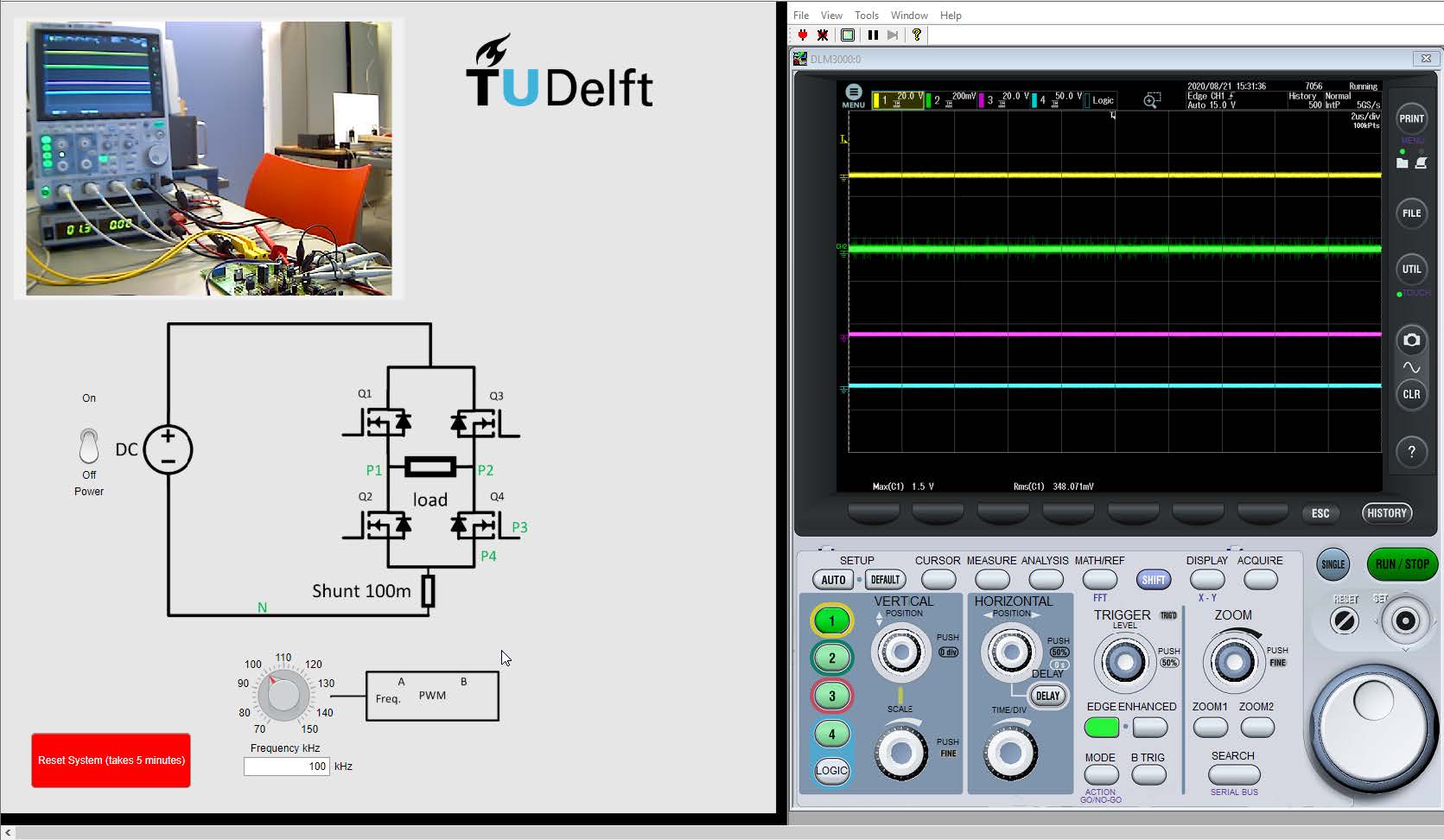
Fig. 1 Remote practical operation panel of assignment 2.#
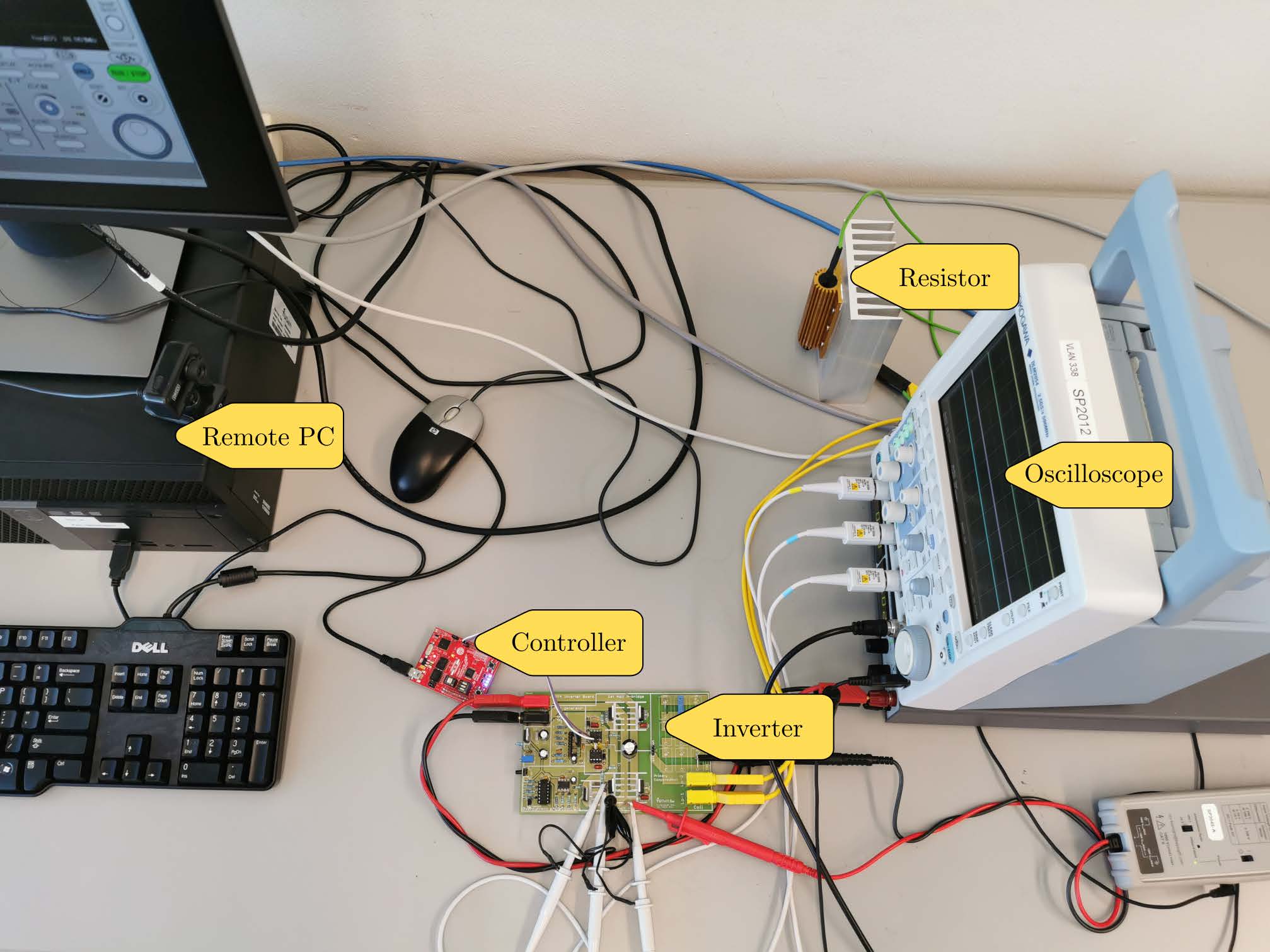
Fig. 2 Remote practical setup of assignment 2.#
The remote practical operation panel and the lab setup behind it are shown in Figure 1 and Figure 2 respectively.
Warning
Please refresh the online practical webpage if the setup becomes unreponsive during the online practical.
Warning
Please do not hit the fullscreen button on the scope interface, otherwise the operation panel will be covered. In case that happens you can hit the ESC key to escape from the fullscreen mode. Please do not try to resize individual windows, use the browser zoom instead to fit your screen better.
On the left part of the remote practical panel, there is a schematic of the inverter reflecting the real lab setup in Figure 2. You are able to turn on/off the setup using the switch on the panel, and change the switching frequency of the inverter using the knob. On the right hand side, there is an oscilloscope measuring four different signals from the inverter. You can interact with the oscilloscope by clicking the knobs or buttons on the oscilloscope interface, like what you do with a normal scope. Three normal probes and one differential probe are used. The measuring points are marked as P1, P2, P3, P4 and N respectively on the left panel. You have to identify between which two points each probe ismeasuring by observing the waveforms.
The outcome of assignment 2 should be filled in section 2 of the practical report of module 1. Please include the following content in section 2 of the report:
Identify where the 4 signals are measured by observing the waveforms while changing the frequency and give your justification;
Explain why a differential probe should be used to measure that specific signal;
Observe the shape of the current going via the inverter and how it changes with changing frequency, and give the reasons why it changes in this way. You can obtain the current waveform by measuring the voltage across the shunt resistor;
Explain why the switches on the same leg (Q1 and Q2, Q3 and Q4) cannot be turned on simultaneously;
Calculate the deadtime (the time interval between one switch turns off and the other switch on the same leg turns on) of the switches by measuring the waveforms. Please also include your calculation procedure.
Tip
You may consider the deadtime and the non-ideal behaviours of the components (e.g. a resistor might show inductive behaviour at higher frequency) to help you answer the questions above.
Assignment 3: compensation of a contactless power transfer system#
Please read
Read the Power Electronics and the Mangetics parts of the reader;
Chapters 8, 9 and 10 of “Engineering Circuit Analysis” by J. David Irwin;
Theoretical background section of this manual.
for background knowledge to carry out this assignment.
Assignment 3 should be done at home without using the online practical setup. In assignment 3, you calculate the performance of a wireless power transfer system with and without compensation capacitors. In Table Table 1 you can findmain parameters of the system. The symbols in the table are according to the notation used in the theoretical background section.
Parameters |
Value |
Parameters |
Value |
|---|---|---|---|
\(L_1\) |
\(185~\mu\mathrm{H}\) |
\(L_2\) |
\(20~\mu\mathrm{H}\) |
\(k\) when aligned |
0.3 |
\(r_1\) |
\(194~\mathrm{m\Omega}\) |
\(r_2\) |
\(88~\mathrm{m\Omega}\) |
\(R\) |
\(8.1~\mathrm{\Omega}\) |
\(V_{in}\) |
\(18~\mathrm{V}\) |
\(f\) |
\(100~\mathrm{kHz}\) |
Warning
The values in the above table are just for you to practice the calculation in Assignment 3. The circuit parameters to be used in Assignment 4 are based on the real system to be measured. The inductance values in Assignment 4 might differ from the table above and might change from year to year. The capacitance in Assignment 4 is set by bypassing one or more capacitors. The resonant frequency should be tuned by yourself accordingly.
The outcome of the assignment will be filled in section 3 of the practical report of module 1. Please include the following content in section 3 of the report:
The power the system is able to transfer and its efficiency without compensation;
Justify why the transferred power and the efficiency are not high;
Calculate required capacitance values on each side to fully compensate the system;
Calculate the theoretical transferred power and efficiency using the calculated compensation.
Assignment 4: measurements of a contactless power transfer system#
You can do assignment 4 once you finish assignment 3. The reservation system and method are the same as those of assignment 2. Please choose EE2E11_module1_assign4 from Select a resource dropdownmenu on the reservation website to reserve the time slot.
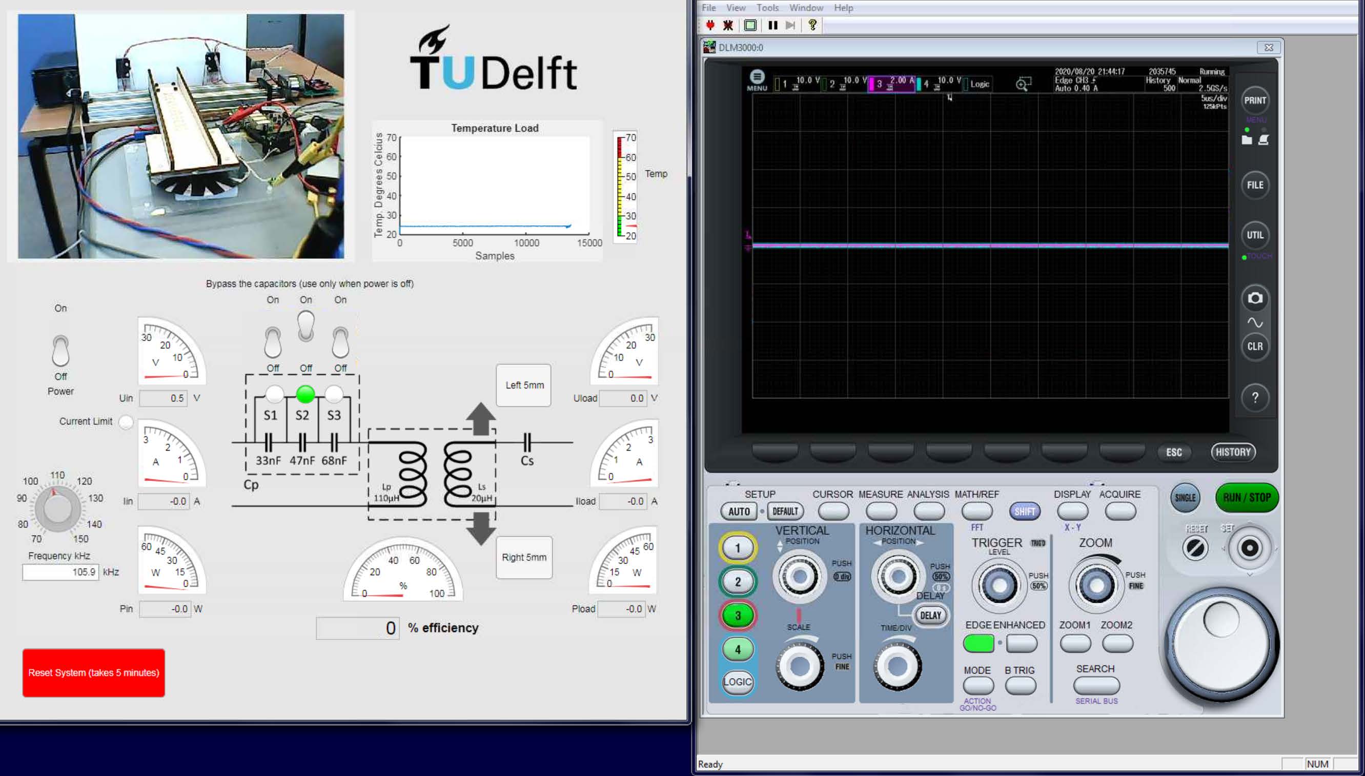
Fig. 3 Remote practical operation panel of assignment 4.#
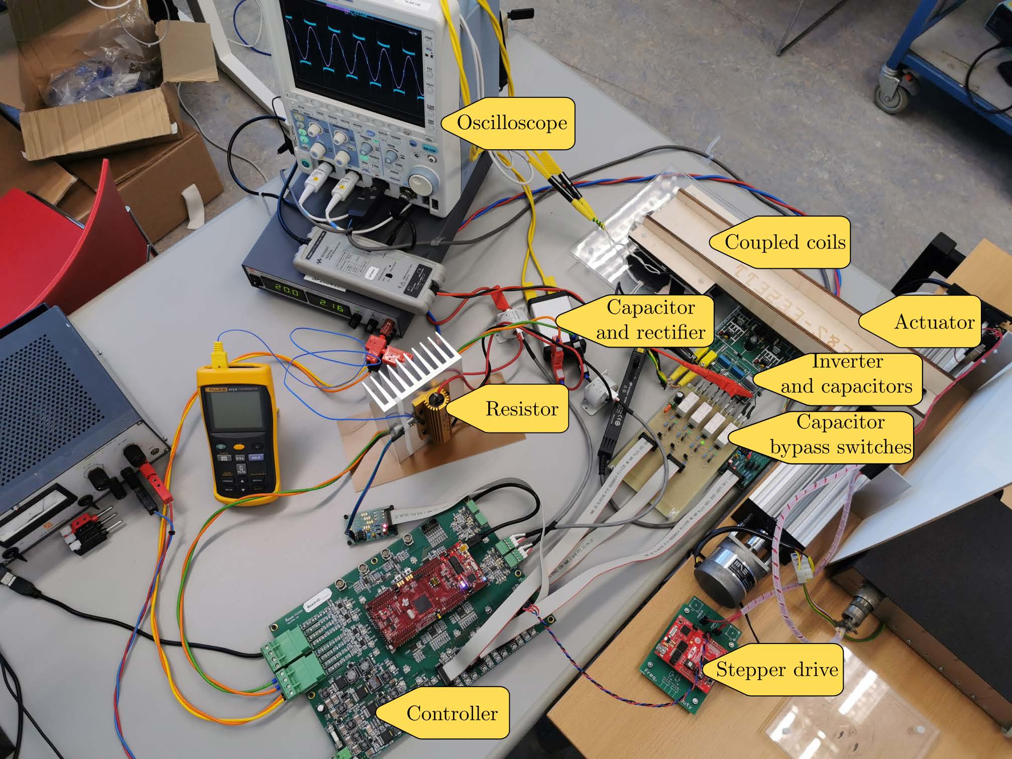
Fig. 4 Remote practical setup of assignment 4.#
Warning
Please take a screeenshot if you want to save the waveform from the oscilloscope. The save function in the oscilloscope does notwork since it only saves to the remote PC, instead of your own computer.
Warning
Please refresh the online practical web page if the setup becomes unreponsive during the online practical.
Warning
Please do not hit the fullscreen button on the scope interface, otherwise the operation panel will be covered. In case that happens you can hit the ESC key to escape from the fullscreen mode. Please do not try to resize individual windows, use the browser zoom instead to fit your screen better.
The remote practical operation panel and the lab setup behind it are shown in Figure 3 and Figure 4 respectively.
You can use the power on/off switch on the operation panel to turn on/off the power of the setup. The knob on the operation panel below the switch can be used to tune the switching frequency of the inverter. In the setup, there are 3 capacitors connected in series between the primary coil and the inverter. You are able to bypass any of them by turning on corresponding switches above the schematic on the operation panel. However, you are only allowed to change the bypass status when the power is off. You can also see that the secondary side of the coupled coils is mounted on an actuator. By clicking the Left 5mm and Right 5mm buttons on the operation panel, you are able to to change the position of the secondary coil, therefore a misalignment between the coils is created, which can be observed from the webcam.
There are three meters measuring corresponding voltage, current, and power at the primary DC side and the secondary DC side respectively. These measurements are done at the DC part of each side (before the inverter and after the rectifier). The total system efficiency from DC to DC is displayed in the meter at the bottom center of the operation panel. Between the three primary side meters and the power switch, there is a light to indicate whether current limit of the system is reached.
Warning
You would not be able to turn on the setup if the over current limit light is on. If it happens you need to change the setup settings to solve the over current problem first before hitting the turn on button.
Please follow the procedure below to do assignment 4.
Make sure the two coils are properly aligned by clicking the Left 5mm and Right 5mm buttons;
Choose the compensation and frequency based on the calculation method practiced in assignment 3. Do not forget to use the real capacitance and frequency values you see from the panel;
Take notes of the measurements;
Fine tune the switching frequency to achieve the highest transfer power, and take notes of your measurements, frequency, and compensation;
Fine tune the switching frequency to achieve the highest efficiency, and take notes of your measurements, frequency and compensation;
Change the misalignment status by moving the secondary coil, repeat 3-4 at three different positions;
After 1-6 have been done, explore how high the power the system can transfer and how high the efficiency can be by tuning the switching frequency, changing the compensation, and misaligning the coils without hitting the current protection. Take notes of your final results.
The outcome of the assignment will be filled in section 4 of the incremental report of module 1. Please include the following contents:
Tables to show your measured results;
Compare the theoretical calculation of the power/efficiency with those you get from measurements. Identify the reasons for mismatches if there are any;
Calculate the mutual inductances at the three different misalignment conditions using the formulae available in Theoretical Background;
Explain why the highest efficiency or the highest power transfer can be achieved under the settings you explored in step 6.
Warning
The voltage/current on the operation panel are measured on the DC sides, so you should not substitute them directly in the formulae derived in the AC circuit.
Tip
You may consider the non-ideal behaviours of the components to help you explain the results, including the switching losses, parasitic resistances of the capacitors, skin effect etc.
Please submit the report for module 1 to Brightspace course page under Assignments -> Practical module 1, final report. The deadline is 1 November, 2023.
Theoretical background: contactless power transfer#
Power electronics#
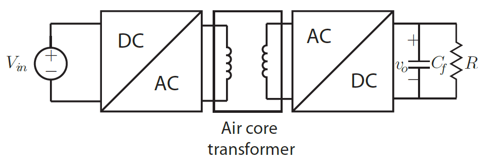
Fig. 5 The DC-DC converter for contactless power transfer.#
The power electronic subsystem of the contactless power transfer system as shown in Figure 5 consists of three main parts, a DC to AC converter (inverter), a high frequency air coupled transformer and an AC to DC converter (rectifier). Furthermore, there are additional sub-circuits for driving the switches, control and circuit protection (not shown in the figure). You must read the preparation documents and design all three components and its subcircuits.
Gate Driver (IRS2001PBF)#
So far in our analysis of power electronic circuits it was assumed that all switches are ideal. This means that they receive some control signal that has no delays and requires no effort to generate. Furthermore ideal switches can switch instantaneously from the on-state to the off-state and vice versa.
Let’s first consider the control signal to the transistors. A MOSFET requires a voltage to be generated between the gate and the source terminals, when this voltage is above a certain level the transistor will switch on and below this threshold the transistor will be in the off state. Although it is true that the transistor can operate in the linear region between the fully on and fully off state (as used in linear audio amplifiers) in power electronic circuits transistors are operated in either the fully on or the fully off state to minimize losses. The MOSFET will be in the fully off state when the voltage between the gate and the source is 0 V and in the fully on state when (according to the datasheet) the voltage is higher than 10 V.
The first problem with the generation of this voltage is the fact that although it is relatively easy to generate the voltages for the two switches on the bottom (since their sources are connected to ground) it is much more difficult to do so for the top switches since their source terminals are not connected to ground and can therefore be at any voltage. A special circuit is needed that can deliver and keep a voltage of 15 V between the source and gate terminals of the topside switches under all operating conditions. This includes the worst case scenario where the source terminals are effectively connected to the positive side of the source (since the top switches are turned on).
Although it is possible to build this gate drive circuit using discrete transistors it is much more convenient to use a dedicated gate drive integrated circuit such as IRS2001PBF. The datasheet of this gate drive circuit is found on Brightspace. This gate drive circuit is able to deliver and keep the required voltage under all operating conditions. Furthermore, the gate drive circuit can deliver a current of 350 mA to the gate of the MOSFET transistor.
Switching Times#
The second assumption concerning the switching elements was that they switch instantaneously from the on-state to the off-state. Ten years ago this assumption would have been pretty bad even at the low power levels that we are investigating. However, technology improved much during the last years. The transistors that can be used for your circuit can switch from the on-state to the off-state in less than 5 ns. That is pretty quick. Consider that light does not even travel 1 meter in 3 ns! This is however not true for all power electronic switching elements, some of the large switches such as the 6.5 kV and 500 A IGBT (a type of transistor) can have a switching time of between 4 and 7 ¹s. However, for your circuit it is safe to assume that the switching time is ideal.
You will have several options available for choosing the switches for the inverter circuit. They differ in switching times and losses when conducting. Think about which is the best choice to keep the losses as low as possible and thus efficiency of the whole circuit as high as possible.
There is one other factor to consider and that is the fact that the control signal takes a certain time to travel from the control board to the MOSFET and again a certain time for the MOSFET to react on the signal. It is possible to calculate this time delay by adding the delay times of theMOSFET and the gate driver together. This data is available on the datasheets.
The PWM Generation and Control Circuit#
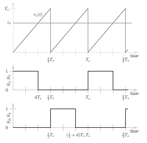
Fig. 6 Generating the PWM switching signals for the full bridge converter.#
There are several methods to generate the PWM signals for a full bridge converter. The easiest method is shown in Figure 6. Again although it is possible to build a circuit to generate these waveforms using transistors and operational amplifiers it is easier to use a dedicated integrated circuit. We will use UC3525 manufactured by Texas Instruments, again the datasheet for this circuit is found on Brightspace.
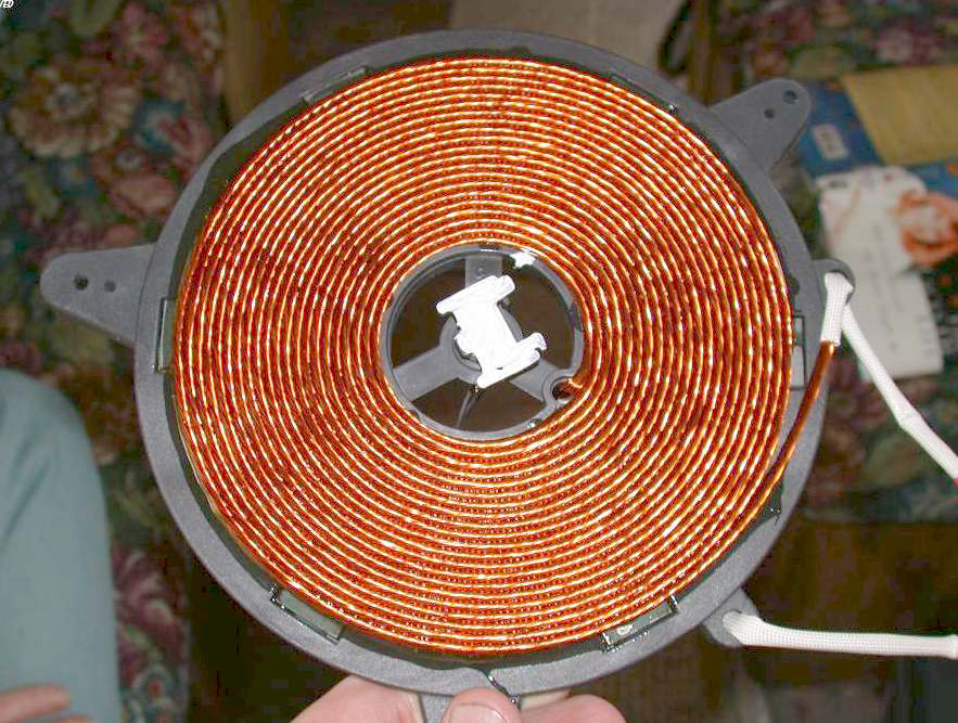
Fig. 7 A contactless power transfer coils.#
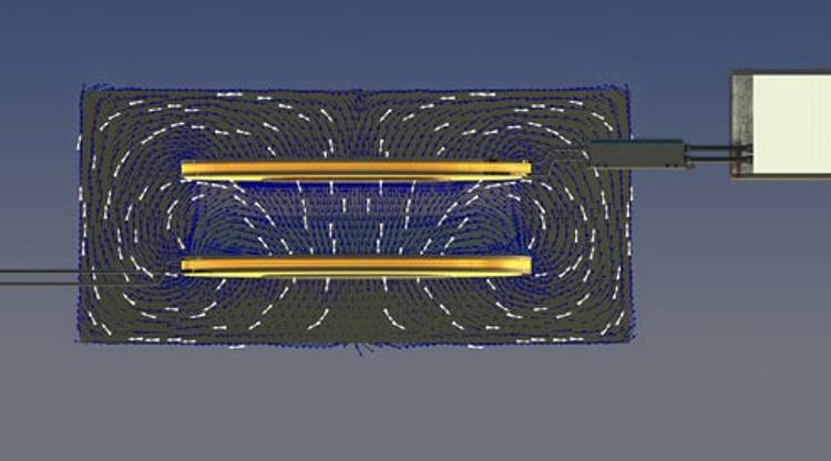
Fig. 8 The magnetic field distribution in the air core transformer.#
Air-coupled transformer#
For the contactless power transfer an air-core transformer will be used. As with any transformer the system consists of two coupled inductors. However, the main difference is the absence of a welldefined magnetic circuit. This lack of a low-reluctance path for the magnetic flux to couple the primary and secondary windings together results in a magnetically loosely coupled system.
Winding of the Coils#
The basic shape of the winding that will be used is shown in Figure 7. Having this flat shape allows for a little more flexibility in the setup of the contactless power transfer. If the coils are made long and slim instead of flat and wide (as the one shown in Figure 7) then the alignment of the coils would be more difficult. To illustrate this point, consider Figure 8, here two coils of the shape of Figure 7 are placed above one another and the distribution of the magnetic flux is superimposed on the image. Although it can be seen that there is a fair amount of flux generated by the coil in the bottom that does not couple with the coil on top, it can also be seen that the relatively flat shape of the coil helps to capture as much flux as possible.
Each group will design and wind their own coils. First consider the design constraints. The inside diameter of both coils should not be smaller than 5cm. A small inside diameter not only limits the ability of the coil to capture flux but the inner winding also contributes little to the inductance. The total inductance of the larger coil should be in the region of around \(\mathrm{100~\mu H}\) and \(\mathrm{20~\mu H}\) for the smaller. A special type of high frequency wire, called Litz wire, that consists of many small strands bound together will be supplied for the coils. The total inductance and the length of wire needed can be estimated using the air-core inductance calculator located at http://www.pronine.ca/spiralcoil. htm using the parameters of the supplied Litz wire. You can now calculate the size of the inductor for different inner diameters and inductance values.
Measurement methods#
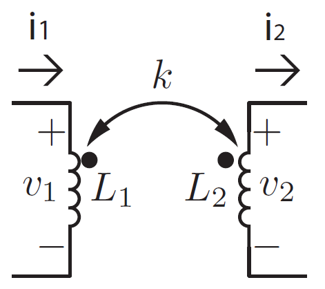
Fig. 9 Two coupled inductors.#
Consider the coupled inductors shown in Figure 9. Let \(L_1\) and \(L_2\) be the self inductance of the two coils and \(M\) be the mutual inductance of the two coils. You already know that we can model this circuit with
where
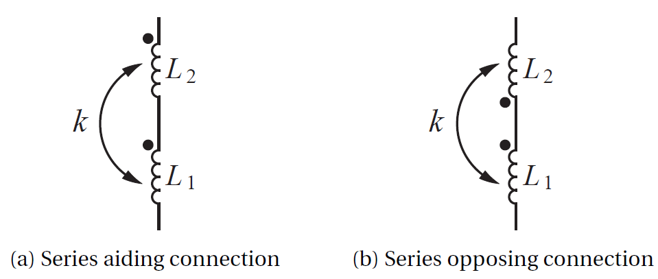
Fig. 10 Series-aiding (a) and series-opposing (b) connection of coupled inductors.#
Consider the circuits shown in Figure 10. The inductors are connected in series in both circuits, however, in the one instance the induced voltages are in the same direction while in the other they oppose one another. Measuring the inductance of these circuits as well as the self-inductances of \(L_1\) and \(L_2\) gives enough information to calculate the coupling coefficient.
Lets define \(L_{s}\) to be the total inductance of the two coils connected in the series aiding configuration. Finally, let \(L_o\) be the total inductance of the two coils connected in the series opposing configuration.
When the two coils are connected in series (irrespective of whether they are connected in the aiding or opposing configuration) they share the same current, \(i\). If \(v_1\) is the voltage across \(L_1\) and \(v_2\) is the voltage across \(L_2\) the following can be written
when the coils are connected in the series aiding configuration. Using these equations one can calculate the voltage across the two coils when connected in the series aiding configuration, \(v_a\), as
Since the voltage across the the two coils connected in the series aiding configuration is related to the total inductance of the two coils as
you now know that
You can prove that for the series opposing connection of the two coils the total inductance of the two coils are
Using these equations you can now calculate the mutual inductance as
and since
you can now calculate the coupling coefficient.
In this discussion you have made a number of simplifying assumptions, most notably you have ignored the winding resistances. Although this simplified model gives you enough information to understand the operation of the system it can not describe all the behaviour of the system, such as the efficiency for example. In the master’s course methods of analysing the resistance and describing it as a function of frequency as well as methods to generate detailed models of the magnetic characteristics will be addressed.
Power transfer characteristics#
Due to the loose coupling of the inductors when the air core is used the operation of the DC-DC converter will be quite different. In a full bridge DC-DC converter with a ferrite transformer the coupling between the two coils is very high and one could ignore the transformer power transfer characteristics. Although it is very difficult to analyse the circuit operation in the time domain using the techniques you have used thus far when analysing power electronic converters you can use a sleight of hand to get you out of trouble. Remember that since the switching waveform of the inverter is periodic you can rewrite the time-domain waveform in the frequency domain using the Fourier series. You can now analyse the operation of the transformer circuit and assume that the source is sinusoidal. Although you theoretically have to calculate the currents and voltages for each and every component of the Fourier series to get the full picture of what will happen when you connect the air core transformer to the inverter you can get a very good idea of how well the transformer is working by investigating only the fundamental frequency component. If the transformer is able to deliver a sensible amount of power at the fundamental component chances are good that it will be able to do so with the full waveform.
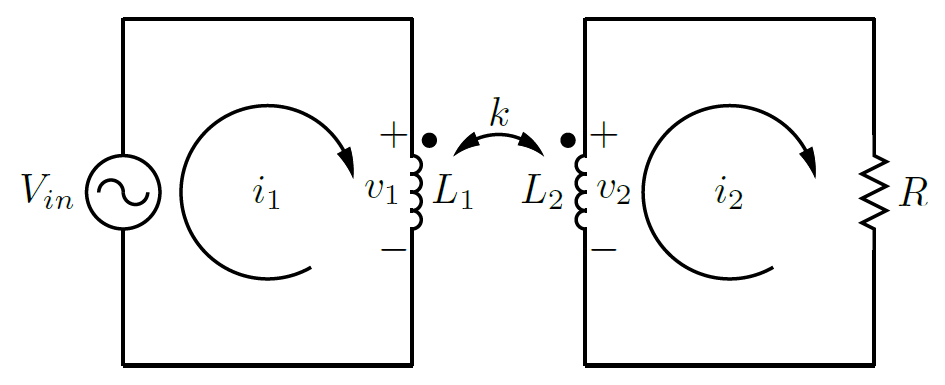
Fig. 11 Basic coupled inductor power transfer circuit.#
Consider the coupled inductor circuit shown in Figure 11. Since you are interested in the fundamental component you can assume that the frequency of the source is 100 kHz. Recall that for the coupled inductors you can write the following equation, in the frequency domain,
Using this expression you can write the Kirchhoff voltage loop law equations for the system in Figure 11 as
By solving these equations we is able to obtain the active power transfer to the secondary side. below 0.4.
We can see very little power is transmitted to the load resistance if the coupling coefficient is low, say below 0.4.
When you include the winding resistances, as in the circuit of Figure 12 the efficiency of the system is very low. You can actually expect that since you can see that the power factor of both systems in Figure 11 and Figure 12 is very low.
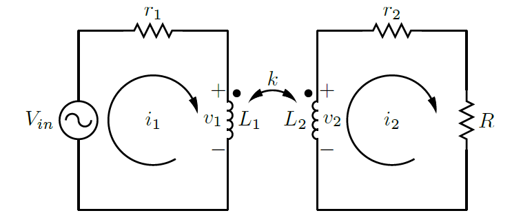
Fig. 12 Basic coupled inductor power transfer circuit.#
Compensation#
In the previous section, while analysing the air-coupled transformer, you have seen that the power transfer characteristics of such a transformer are poor, because the power factor of both sides in Figure 12 is very low. In this assignment, you need to look for a solution to this problem.
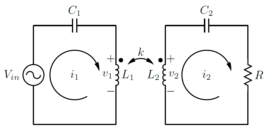
Fig. 13 Basic compensated coupled inductor power transfer circuit.#
A common approach to improve the power factor of the inductive circuit is adding compensation capacitors. As shown in Figure 13, capacitors C1 and C2 are added in series to the primary and secondary circuit respectively. Similarly to (11)-(13), by applying the Kirchhoff’s law, you can write
The Thévenin’s equivalent impedance of the primary side is calculated from (15) as
To transfer maximum power with certain voltage and current, the Thévenin’s equivalent impedance should only have real component. Therefore, the two \(j\) components in (16) both should be 0, which gives
As you can see, \(L_1\) and \(L_2\) now resonant with \(C_1\) and \(C_2\) respectively at frequency \(f\). Then the primary side Th’evenin’s equivalent impedance becomes
Now let’s calculate the power transfer efficiency of the above fully compensated case, the primary current can be written as
Substitute (19) and (17) into (15) you can get the secondary current is
The output power is calculated as
As we can see from (18) to (21), when the load and the input voltage are fixed, the current in the coils and the transferred power is determined by the switching frequency and the mutual inductance, hence the power transfer efficiency. In practice the switching frequency is often tuned according to the load to realize a high efficiency power transfer by the so-called ”impedance matching”.
The other problem for the fully compensated case is the misalignment. Consider what would happen if the secondary is removed from the primary or the two coils are heavily misaligned. The mutual inductance \(M\) becomes close to 0. According to (18) and (19), the primary side current will be extremely high since the equivalent impedance is too low. Large current may damage the inverter circuit. Therefore a current sensor is added to the main current path. It measures the current and protects the inverter in case of overcurrent.